
Professional PCB manufacturing and assembly
Building 6, Zone 3, Yuekang Road,Bao'an District, Shenzhen, China
+86-13410863085Mon.-Sat.08:00-20:00

PCB production process flow 2
PCB engineering production
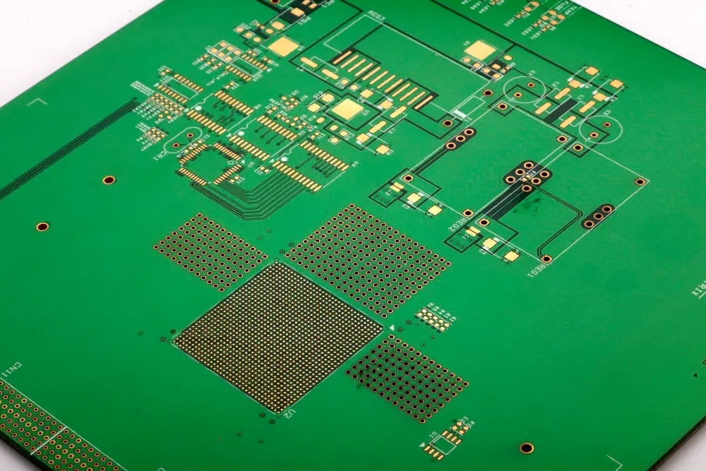
For the production of PCB, because many designers do not understand the production process of PCB, the circuit diagram designed by them is only the most basic circuit diagram and cannot be directly used for production. Therefore, it is necessary to modify and edit the circuit file before actual production. It is not only necessary to make a film chart that can be suitable for the production process of our factory, but also necessary to make corresponding punching data, mold opening data, and other data useful for production. It is directly related to future production projects. All these require engineering technicians to understand the necessary production process and master the relevant software production, including common circuit design software such as Protel, Pads2000, Autocad, etc., and be familiar with necessary CAM software such as View2001 and CAM350; GCCAM, etc. CAM shall include PCB design input, which can edit, correct, repair and assemble circuit graphics, use disk as the medium material, and output automatic data of photo drawing, drilling and detection.
Basic requirements for PCB engineering fabrication
The level of PCB engineering production can reflect the design level of the designer, as well as the production process capability and technical level of the PCB manufacturer. At the same time, as the PCB engineering production integrates computer aided design and auxiliary manufacturing, extremely high precision and accuracy are required, otherwise the electrical performance of the final on-board electronic products will be affected, and errors may be caused in serious cases, which will lead to the scrapping of the whole batch of PCB products, delay the manufacturer's contract delivery time, and suffer economic losses. Therefore, as a PCB engineer, you must always bear in mind that you have a great responsibility. Don't take it lightly. Be careful, careful, and serious. When processing PCB design files, you should carefully check:
Does the received document conform to the rules made by the designer? Can it meet PCB manufacturing process requirements? Are there positioning marks?
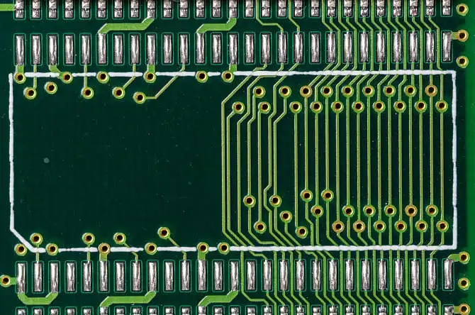
Is the line layout reasonable? Whether the distance between line and line, line and component pad, line and through-hole, component pad and through-hole, through-hole and through-hole is reasonable and can meet the production requirements. Is there any conflict between components in 2D and 3D space?
Is the size of printed board consistent with the processing drawing? Whether the graphics (such as icons and labels) added in PCB graphics will cause signal short circuit.
Edit and modify some undesirable lines.
Is there a process line on the PCB? Whether the resistance welding meets the requirements of the production process, whether the resistance welding size is appropriate, and whether the character mark is pressed on the device pad to avoid affecting the electrical installation quality. Wait
Generation of photo data
1. Patchwork
The PCB design is completed because the PCB shape is too small to meet the production process requirements, or a product is composed of several PCBs, so it is necessary to assemble several small boards into a large board with an area meeting the production requirements, or to assemble multiple PCBs for a product to facilitate the production of electrical equipment. The former is similar to the stamp board. It can not only meet the PCB production process conditions, but also facilitate the electrical installation of components. It is very convenient to separate them when using; The latter is to assemble several sets of PCB boards of a product together, which is convenient for production and is also convenient for a complete set of products.
2. Generation of optical drawing data
The base of PCB production is film base. In the early stage of making a film base, it is necessary to make a film base first, and then use the base to take photos or copy. The accuracy of the base drawing must be consistent with the requirements of the printed board, and compensation for the deviation caused by the production process should be considered. The base drawing can be provided by the customer or made by the manufacturer, but both parties should cooperate and negotiate closely to make it meet the user's requirements and adapt to the production conditions. If the user provides the base drawing, the manufacturer shall inspect and approve the base drawing, and the user can evaluate and approve the original version or the first printed board product. The base map is made by hand drawing, mapping and CAD drawing. With the development of computer technology, the PCB CAD technology has made great progress, and the PCB production process level has also been rapidly improved to the direction of multi-layer, thin wire, small aperture, and high-density. The original film plate making process can no longer meet the design needs of PCB, so photo painting technology has emerged. The number of PCB graphics designed by CAD can be directly transferred by using photo plotter
The files are sent to the computer system of the photo plotter, which controls the photo plotter to draw graphics directly on the negative film using light. Then, the film base is obtained by developing and fixing. The photo painting technology is used to make the printed circuit board film base plate, which is fast, accurate, and of good quality. It also avoids the human errors that may occur when manually mapping or drawing the base plate, greatly improves the work efficiency, and shortens the production cycle of the printed circuit board. Using our laser photo plotter, we can complete the work that many people used to do for a long time in a very short time, and the thin wires and high-density plates drawn by it are incomparable to manual operation. According to the different structures of laser photo plotters, they can be divided into flat plate type, internal drum type and external drum type. Yuzhiguang's series of photo plotters are all internationally popular outer drum type.
The standard data format used by photo plotter is Gerber-RS274 format, which is also the standard data format of PCB design and production industry. The name of Gerber format is quoted from the American Gerber Company, the pioneer of photo plotter design and production.
The generation of photo drawing data is to convert the design data generated by CAD software into photo drawing data (mostly Gerber data), modify and edit them through CAM system, and complete photo drawing preprocessing (plate assembly, mirror image, etc.) to meet the requirements of PCB production process. Then, the processed data is sent to the photo plotter, which is converted into raster data by the Raster image data processor of the photo plotter. This raster data is sent to the laser photo plotter through the high speed compression and restoration algorithm to complete the photo painting.
3. Photo data format
The photo data format is developed based on the data format Gerber data of the vector photo plotter, and has expanded the data format of the vector photo plotter, and is compatible with HPGL HP plotter format, Autocad DXF, TIFF and other special and general graphics data formats. Some CAD and CAM developers have also extended Gerber data.
Here is a brief introduction to Gerber data:
The official name of Gerber data is Gerber RS-274 format. Each symbol on the code disk of the vector photo plotter has a corresponding D-CODE in Gerber data. In this way, the photo plotter can control and select the code disk through the D code, and draw the corresponding graphics. List the shape and size of the symbols corresponding to D code and D code to get a D code table. This D code table becomes a bridge from CAD design to photo drawing machine using this data. The user must provide the corresponding D code table while providing Gerber photo data. In this way, the photo plotter can determine which symbol disk should be used for exposure according to the D code table, so as to draw the correct figure.
A D code table should generally include the D code, the shape and size of the code disk corresponding to each D code, and the exposure method of the code disk. Taking a D code table of Protel, the most commonly used electronic CAD software in China, as an example, its extension is. APT, which is an ACSII file, and can be edited with any non text editing software.
In Gerber RS-274 format, in addition to defining the symbol disk with D code, D code is also used for exposure control of photo plotter; In addition, some other commands are used to control and run the photo plotter. The Gerber data format generated by different CAD software may have some minor differences, but the overall framework is Gerber-RS0274 format.
4. Computer Aided Manufacturing (CAM)
Computer Aided Manufacturing (CAM), which is called Computer Aided Manufacturing in English, is an advanced technology controlled by Computer to complete production. With the development of computer technology and the appearance of laser plotter, the computer aided manufacturing technology of PCB has been used. CAM technology makes the design and production of printed circuit board go to a new level, and some functions that could not be realized in the past can be realized. Various CAM systems can generally process photo data (Gerber data), eliminate various defects in the design, make the design easier to produce, and greatly improve the production quality.
The main functions of the CAM system are as follows:
1. Editing function:
1) Add pads, lines, arcs, characters and other elements to generate water drop pads.
2) Modify pad and line size.
3) Move pads, lines, dimensions, etc.
4) Delete various drawings, and automatically delete pads and air vents without electrical connection.
5) Automatic treatment of solder leakage.
6) Screen printing character cover pad automatic processing.
2. Composition, rotation and mirroring
3. Add various locating holes
4. Generate NC drilling data and milling profile data
5. Calculation of conductor copper foil area
6. Other relevant data
In the microcomputer CAM system, the representative is the View2001 software developed by Lavenir Company. View2001 is a microcomputer CAM system composed of a series of practical photo data processing programs, which can run under DOS platform and DOS window of WINDOWS'9X. It contains several main programs. Here is a brief introduction to V2001.EXE.
V2001.EXE is a Gerber data editing software with relatively complete functions. It can read various types of Gerber data files, including Gerber basic formats and various Gerber extended formats. It supports Gerber data and D code table generated by various CAD systems, and edits and modifies them, and can process up to 99 layers of data at the same time. V2001 can recognize the D code table generated by more than 10 CAD and CAM systems, such as Lavenir, PADS, P-CAD, ORCAD, Tango, Protel, Mentor, and is easy to operate.
The main functions of V2001 are:
1) Delete, move, add lines, pads, arcs, characters and other graphics.
2) Simple composition.
3) Transfer and transformation of graphics and data between layers.
4) Character processing: automatically clear the characters on the overlapping part of the character screen layer and the pad.
5) Soldering resistance treatment, automatic processing of welding resistance of missing lines.
6) Solder paste screen processing, automatically generate solder paste screen graphics of surface mounted components.
V2001 can well process photo data, has strong strain capacity, and can process Gerber data generated by various CAD software. However, the user interface is not friendly, and the software operation uses command mode. There are many commands that need to be memorized, and they are more complex, making it difficult for beginners to learn. But once mastered, it can easily meet the needs of most of the current PCB engineering production.
During the training, the trainees should understand the specific modification and editing of documents provided by customers in V2001, mainly including:
1) Convert Gerber data files from source files. For data conversion of Gerber files, see the Student Manual of Yuzhiguang.
2) First, check whether each layer has a board layer frame (enclosure).
If yes, check whether the thickness of the frame meets the requirements of the production process. Generally, the current double-sided plate shall be at least 0.15 mm (6 mil); The single panel shall be at least 0.2mm (8mil); Or edit and modify according to the information provided by the customer.
If not, check whether there is missing transfer. The missing transfer needs to be converted again. You can also copy the border from other layers with borders.
3) Convert all elements that can be converted into FLASH pads as much as possible into pads (optional).
4) Check whether the line width and spacing of the line layer meet the production process requirements. Generally, the line width and spacing of the line layer of the current double-sided board shall be at least 0.15 mm (6 mil); The line width and spacing of the line layer of the single panel shall be at least 0.2mm (8mil); Or edit and modify according to the information provided by the customer.


Just upload Gerber files, BOM files and design files, and the KINGFORD team will provide a complete quotation within 24h.