
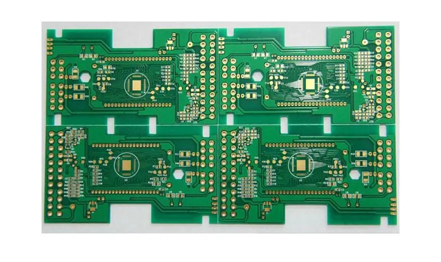
Professional PCB manufacturing and assembly
Building 6, Zone 3, Yuekang Road,Bao'an District, Shenzhen, China
+86-13410863085Mon.-Sat.08:00-20:00

Manufacturing process flow of flexible circuit board
Flexible Printed Circuit (FPC) can be bent, wound and folded freely. FPC is processed with polyimide film as the base material, which is also called flexible board or FPC in the industry The process flow of FPC is divided into double-sided FPC process flow and multi-layer FPC process flow according to different layers. FPC soft board can withstand millions of times of dynamic bending without damaging the wire, can be arranged arbitrarily according to the space layout requirements, and can move and expand freely in three-dimensional space, so as to achieve the integration of component assembly and wire connection; Flexible circuit board can greatly reduce the volume and weight of electronic products, which is suitable for the development of electronic products in the direction of high-density, miniaturization and high reliability.
As more and more mobile phones use flip structures, flexible circuit boards are also increasingly used.
According to the combination mode of base material and copper foil, flexible circuit boards can be divided into two types:
Adhesive flexible plate and adhesive free flexible plate.
The price of adhesive free flexible board is much higher than that of adhesive flexible board, but its flexibility, adhesion between copper foil and substrate, flatness of bonding pad and other parameters are also better than that of adhesive flexible board. Therefore, it is generally only used for those occasions with high requirements, such as COF (CHIP ON FLEX, mounting bare chips on flexible boards, and high requirements for pad flatness).
Because of its high price, most of the flexible boards currently used in the market are still flexible boards with glue.
Next, we will introduce and discuss flexible plates with glue. As the flexible plate is mainly used in the situation where bending is required, if the design or process is unreasonable, it is easy to produce microcracks, open welding and other defects. The following is about the structure of flexible circuit board and its special requirements in design and process.
Structure of flexible plate
According to the layers of conductive copper foil, it can be divided into single-layer board, double-layer board, multi-layer board, double-sided board, etc.
Single layer plate structure: the flexible plate of this structure is the flexible plate of the simplest structure. Generally, the base material+transparent adhesive+copper foil is a set of purchased raw materials, while the protective film+transparent adhesive is another kind of purchased raw materials. First, the copper foil needs to be etched to obtain the required circuit, and the protective film needs to be drilled to expose the corresponding bonding pad. After cleaning, use the rolling method to combine the two. Then, the exposed bonding pad shall be electroplated with gold or tin for protection. In this way, the big board is ready. Generally, small circuit boards should be stamped into corresponding shapes.
There are also those who print solder mask directly on copper foil without using protective film. This will lower the cost, but the mechanical strength of the circuit board will become worse. Unless the strength requirement is not high but the price needs to be as low as possible, it is better to apply the protective film.
Double layer board structure: When the circuit is too complex, the single layer board cannot be wired, or copper foil is required for grounding shielding, double layer board or even multilayer board is required.
The most typical difference between multilayer board and single-layer board is that the via structure is added to connect each layer of copper foil. Generally, the first processing process of substrate+transparent adhesive+copper foil is to make vias. First, drill holes on the base material and copper foil. After cleaning, coat a certain thickness of copper, and then the through-hole is ready. After that, the manufacturing process is almost the same as that of single layer board.
Double sided board structure: both sides of the double sided board have pads, which are mainly used for connection with other circuit boards. Although its structure is similar to that of single layer board, its manufacturing process is very different. Its raw materials are copper foil, protective film and transparent adhesive. First, drill holes on the protective film according to the position requirements of the bonding pad, and then stick the copper foil. After the bonding pad and lead are corroded, stick another protective film with drilled holes.
Material performance and selection method
(1) . Base material:
The material is polyimide, which is a high temperature resistant and high-strength polymer material. It is a polymer material invented by DuPont. The polyimide produced by DuPont is named KAPTON. In addition, you can also buy some polyimides produced in Japan, which are cheaper than DuPont.
It can withstand the temperature of 400 ℃ for 10 seconds, and the tensile strength is 15000-30000PSI.
twenty-five μ The m-thick substrate is the cheapest and most widely used. If the circuit board needs to be hard, 50 should be selected μ M substrate. On the contrary, if the circuit board needs to be soft, choose 13 μ M substrate.
(2) Transparent adhesive of base material:
It is divided into epoxy resin and polyethylene, both of which are thermosetting adhesives. The strength of polyethylene is relatively low. If you want the circuit board to be soft, choose polyethylene.
The thicker the substrate and the transparent adhesive on it, the harder the circuit board is. If the circuit board has large bending area, try to select thinner substrate and transparent adhesive to reduce the stress on the copper foil surface, so that the copper foil has less chance of microcracks. Of course, for such areas, single-layer boards should be selected as far as possible.
(3) Copper foil:
It is divided into calendered copper and electrolytic copper. Calendered copper has high strength and bending resistance, but its price is expensive. Electrolytic copper is much cheaper, but its strength is poor and it is easy to break. It is generally used in occasions with few bends.
The thickness of copper foil shall be selected according to the minimum width and minimum spacing of lead wires. The thinner the copper foil, the smaller the minimum width and spacing that can be achieved.
When selecting calendered copper, pay attention to the calendering direction of copper foil. The rolling direction of copper foil shall be consistent with the main bending direction of circuit board.
(4) Protective film and transparent adhesive:
Similarly, 25 μ The protective film of m will make the circuit board harder, but the price is cheaper. For circuit boards with large bending, it is better to select 13 μ M protective film.
Transparent adhesive is also divided into epoxy resin and polyethylene. The circuit board using epoxy resin is relatively hard. After hot pressing, some transparent adhesive will be extruded from the edge of the protective film. If the size of the pad is larger than the opening size of the protective film, the extruded adhesive will reduce the size of the pad and cause its edge to be irregular. At this time, try to choose 13 μ M thick transparent adhesive.
(5) Pad coating:
For the circuit board with large bending and some bare pads, the electroplated nickel+chemical gold coating shall be adopted, and the nickel layer shall be as thin as possible: 0.5-2 μ m. Chemical gold layer 0.05-0.1 μ m。
Shape design of pad and lead
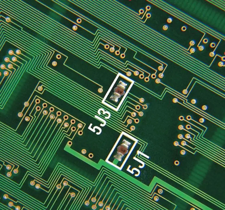
(1) . SMT pad:
——Common pad:
Prevent the occurrence of microcracks.
——Reinforced pad:
If the pad strength is required to be very high or reinforced design is required.
——LED pad:
Due to the high position requirements of LED and the force often applied during the assembly process, its pad needs to be specially designed.
——Pad of QFP, SOP or BGA:
Due to the large stress of the pad on the corner, the reinforced design is required.
(2) . LEADS:
——In order to avoid stress concentration, the lead wire shall avoid right angle corner and adopt circular arc corner.
——The lead near the corner of the circuit board shall be designed as follows to avoid stress concentration:
Design of external interface
(1) Design of circuit board at welding hole or plug:
As the stress of welding hole or plug is large during the insertion operation, the reinforced design shall be made to avoid cracks.
Reinforcing plate is used to increase the hardness of the welding hole plug of the circuit board. The thickness is generally 0.2-0.3mm, and the material is polyimide, PET or metal. For pad coating, it is better to choose electroplated nickel+hard gold for plug and electroplated nickel+chemical gold for solder hole.
(2) Design of hot pressing welding position:
It is generally used for the connection of two flexible boards or flexible boards and hard circuit boards.
If the circuit board needs to be bent near the hot pressing welding area, the polyimide tape or glue shall be pasted on the area for protection to avoid the root of the pad breaking.
(3) Design of ACF hot pressing position:
Design of punching holes and small circuit board corners (see Table 3)
Design for SMT:
(1) . Direction of components:
The length direction of the element shall avoid the bending direction of the flexible plate.
(2) Large QFP or BGA shall be pasted with reinforcing plate on the back of flexible plate or filled with glue under IC.
The material of the stiffening plate is FR4, the thickness is more than 0.2mm, and the area is 0.5mm larger than the outer edge of the element.
(3) Two positioning holes shall be made at the position near the edge of the flexible plate. It is also necessary to make two identification pads for mounting, with a diameter of 1mm and a distance of at least 3.5mm from other pads. The surface is gold-plated or tinned with good flatness.
(4) If the large flexible board is composed of many small boards, each small board should be made with a ring (inner diameter 3.2 mm) of bad circuit board identification pad. If the small circuit board is damaged, the identification pad can be blackened with a black marker to avoid future operations.
(5) The minimum distance between components and the edge of the circuit board is 2.5 mm, and the minimum distance between components is 0.5 mm.
(6) There shall be no via under the component, because the flux will flow through the via and cause pollution.
Design for electrical performance
(1) Relation between maximum current and line width, line height: (see table)
(2) Impedance and noise control:
——Use transparent adhesive with strong insulation, such as polyethylene. Avoid using epoxy resin.
——In high impedance or high frequency circuits, the distance between the conductor and the ground plate should be increased.
——The above design methods can also be adopted:
Special design of SMT process
(1) Positioning method in solder paste printing and patch process:
Because the flexible board is thin and flexible, if the edge of the circuit board is used for positioning, the positioning accuracy is poor. Positioning holes shall be used for positioning. In order to avoid the leakage plate when printing solder paste, the support plate with spring pin shall be used.
(2) The solder paste, patch and heating furnace shall be printed until the visual inspection is completed, and the support plate shall be used to fix the whole process. In order to avoid damage to the solder joints during operation.
Flexible circuit board manufacturers often use some PCB design software to produce flexible circuit boards, such as POWERPCB, DXP, 99SE, AUTOCAD and other PCB design and wiring software. PCB design software can generally download various versions on the Internet. In addition, CAM350 and genesis2000 are commonly used engineering aided design software by manufacturers.
Perforated copper plating for PCB electroplating
Oct 30,2022


Just upload Gerber files, BOM files and design files, and the KINGFORD team will provide a complete quotation within 24h.