
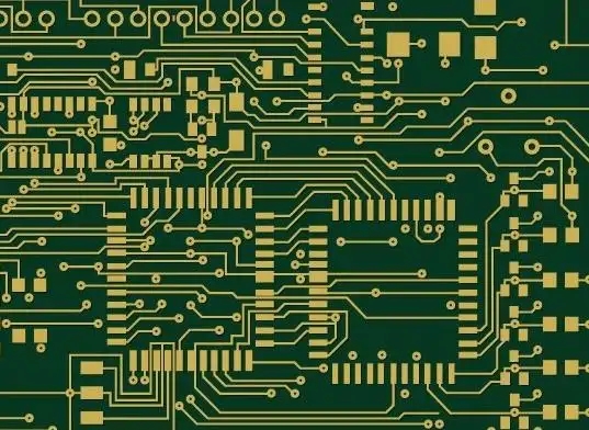
Professional PCB manufacturing and assembly
Building 6, Zone 3, Yuekang Road,Bao'an District, Shenzhen, China
+86-13410863085Mon.-Sat.08:00-20:00

Surface treatment of lead-free soldering for circuit board
The arrival of lead-free soldering for circuit boards has become an inevitable trend. In addition to the replacement of solder, the surface solderability of solder pads, through-hole or part feet must also be changed accordingly. From all aspects, in addition to the OSP and silver immersion described above, lead-free soldering is bound to have a new situation, and many other PCB soldering methods such as tin immersion and bismuth immersion have also been developed.
1、 Immersion Tin
(1) Reaction principle and problems
The circuit board tin dipping has been used in the PCBA industry for many years, but the high temperature bath solution with a simple formula in those years could only last for one week (due to too much invalid tetravalent tin). The dip tin coating is not only very thin and gray, but also has poor solderability. Generally, in ordinary acidic solutions, the electrokinetic order of Cu is+0.342V, while that of divalent Sn is -0.138V. It is certainly impossible to have a "copper dissolution and tin precipitation" against the natural displacement reaction in comparison with the low and high. However, if Thiourea is added to the bath solution, the situation of high and low will be reversed immediately, and then a tin layer will be plated on the copper surface.
The traditional gray tin is a direct replacement reaction of copper dissolution and tin deposition, while the new white tin is a film of organic copper complex on the bare copper surface first, and then indirectly to replace the tin deposition.
2) Improvement and mass production of white tin
The thickness of tin layer obtained by this Self Iimiting exchange dip reaction (stannous sulfate or stannous chloride) is about 0.1-1.5 μ M (at least 1.5 "m for multiple welding, and the residual tin thickness after IMC replacement must be more than 0.3 m). This thickness is directly related to the concentration of stannous ions in the bath solution, temperature, and porosity of the coating. When the copper content in the bath solution is too high, it may deposit and precipitate together with tin, which will certainly have a negative impact on the solderability.
Comparison of the area of tin paste after aging of five treatments:
In order to deeply understand the deterioration of solderability of general tin dipping tin and FST white tin after aging, the tin spraying plate is taken as the standard test reference plate, and white tin and three brands of gray tin dipping are deliberately put under the same conditions for aging; Then, the solder paste is printed and fused, and the size of its spreading area is compared with SEM to learn the change process of solderability. From the figure, it can be seen that the solder of white tin aged under three conditions can still be kept in good condition.
(3) Management of mass production
When white tin is deposited on the copper surface, of course, there must be a lot of copper dissolved into the bath, and there must also be a co deposition effect, which will inevitably have a negative impact on the subsequent solderability. Therefore, the bath must remove copper (the upper limit is 13.7 g/l). As the tin that can be plated in the bath solution exists as divalent ions (Sn++), there will definitely be insoluble substances of turbid and ineffective tetravalent tin in the high-temperature flow operation. Therefore, removal of copper and tetravalent tin has become the normal work of I-Sn.
2 Cu +S n++ —> 2Cu+ +Sn
This cuprous ion is then complexed and mistaken by thiourea (Tu) and methyl sulfonic acid, and becomes a complex ion of formula (Cu (Tu)+2)+MSA.
This picture shows the refrigeration equipment designed by Ato Technology and installed on the tin dipping production line, which can reduce the range of copper dissolution by 8-10g/l and extend the service life of CaO liquor by up to 17MTO
(4) . Hidden worries of tin dipping
As the tin dipping process is carried out on the green paint rear panel, there should be no negative impact on the appearance of the green paint. Unfortunately, the high-temperature bath solution of the new white tin still contains two strong chemicals, namely thiourea and MSA. The mass production experience will almost cause the discoloration of the green paint and even the side corrosion floating (the micro corrosion before S/M can be strengthened to improve it); Although shortening the operation time can lighten the terrible scene, it is also easy to oxidize due to insufficient thickness, and with the acceleration of the formation of IMC, the solderability will certainly be greatly reduced. What is more troubling is that such strong chemicals infiltrate into the green paint body or crevice. Once they are not cleaned completely, the ionic pollution crisis will be a terrible nightmare for high-level boards and books. However, Ormerod, a researcher, claimed that the residual ions in its flat solderable white tin process (FST, the trade name of Dexter) were quite few, averaging only 0.87 μ G/in2, much lower than 28.8 of tin spraying μ g/in2 。
The problem of "tin whiskers" is the most troubling part of tin dipping (detailed in another long article in this issue), but from the literature, it seems that the cylinder is not as serious as bright tin electroplating; And if compared with the a large number of the solders close to pure tin, thin surface treatment is certainly not a villain. If all the above three problems can be overcome, white tin immersion will surely become the number one contributor to lead-free welding.
2、 Bismuth Immersion Bismuth
The price of bismuth metal is not expensive, only about 80% of the price of tin. Generally, the melting point of solder with bismuth can be greatly reduced, which is quite favorable. However, because bismuth is very sensitive to lead, once bismuth content appears in the current tin lead solder, it is likely to form a three-phase eutectic alloy (8Sn-52-40Bi) with local melting point (mp) reduced to only 95 and C, and the porosity is very large, which will lead to insufficient strength of the solder joint, even a common "bismuth crack", which will inevitably lose its color in practical value. Now when singing lead-free, bismuth's troubles are certainly gone.
Although bismuth is added to the solder cartridge, if it is only used for the weldable treatment of the surface of the welding pad, it seems that the cartridge will not hurt if the proportion of the solder joint is very small. This kind of bismuth dip coating can be completed within 1-2 minutes in 500 C bath solution, and the bismuth layer obtained is uniform dark gray. After high temperature aging, the copper color appears slightly, which may be caused by the diffusion of bottom copper atoms. However, there are few materials and suppliers for bismuth immersion plating, which must be related to the insufficient strength of solder joints.
The solderability of bismuth dip plating is good, its hole filling ability is better than that of silver dip plating, and its dependence on flux activity after multiple high temperatures is not as direct and urgent as OSP. The reason is that the OSP protective film after high temperature aging can only be pushed away by a strong active flux and exposed to clean bare copper to complete welding after excessive oxidation and damage aging. The following figure is a comparison of the two in terms of PTH socket welding hole filling capacity (aperture 22-62mil) under the treatment of II different kinds of non cleaning fluxes. The organic acid (OA) strong active flux is used as the control group. From the data, it can be seen that the solderability of bismuth layer is indeed much better than that of OSP.
As for the spreading force surface of solder paste fusion welding, its non aging and aging diffusion resistance are also similar, and the results must be close to those of the other three kinds of coatings. Even after multiple thermal cycle reliability tests, the failure rate of poor tin adhesion is only slightly inferior to that of tin spraying.
This is a comparison of the through hole tin coating rate of two kinds of wave soldering boards with surface treatment after the treatment of 11 different fluxes and oA organic acid respectively. From this experiment, it can be seen that bismuth immersion plating not only has good solderability, but also is not very picky about the formula of flux.
3、 Nickel and Gold Electroplating
Nickel gold electroplating has been used in PCB industry for many years; The acid hard gold is mostly processed on the edge of the plate as the Contact Connection. The thickness of such bottom nickel is about 100-200 "m, and the thickness of gold layer on the surface is about 30" m. Neutral soft gold is used for wire bond processing, such as COB manufacturing processes such as BGA or CSP. Its front side is used for die attach of wafers. The required nickel thickness is usually 200 μ Above m, gold thickness is about 30-50 μ m。 However, the electroplated nickel gold on the reverse side of such packaging carrier plate can also be used for welding. Sometimes it is also applied to the weldable treatment of the part foot surface. Many expensive parts or earlier IC pins or military electronic products almost always use nickel plated gold.
In fact, the solderability and solder joint strength of electroplated nickel gold are not better than those of other treatments, and sometimes they are worse. The reason is that at the moment of welding, the gold component will quickly melt into the solder joint. The real solder joint is Ni4Sn, IMC grown on the nickel surface. The thicker the gold layer is, the more gold will be melted into the solder joint. As long as the weight ratio exceeds 3%, poor brittleness will occur; The smaller the area of welding pad, the more unfavorable it will be. Therefore, it is an unwise decision to use nickel plating for welding. The reason why BGA or CSP carrier plates use nickel gold plating as welding treatment is due to the fact that the other plate must be wired. It is convenient for one object dual-use manufacturing process. To be honest, it is not only unprofessional to use electroplated nickel gold for welding, but also the cost is far beyond the cost of lead-free soldering.
4、 Other weldable treatment of plate surface
The solderable treatment of lead-free welding, in addition to the above common and possibly mass production, has many methods in other literatures or in the experimental stage. Here we introduce four treatment methods that are not mentioned in the foreword, such as: electroplating lithium with immersion gold, electroplating lithium with gold, electroplating nickel without lithium gold (which has become increasingly popular at present), electroplating or electroplating nickel without tin, etc. However, due to the cost and practicality, the opportunities are still small.
5、 Weldable treatment of part feet
The weldable treatment layer of the metal foot surface of the part does not need to be reflow like PC B, so the metal surface of lead or lead alloy is rarely used. The heads of many parts or parts are always made of tinnous sulfate type electroplating pure tin. In recent years, electrotinning with methanesulfonic acid (MSA) formula was also popular, and the resulting coatings were directly covered on the copper or copper alloy substrate. The method can be used for hanging plating or barrel plating of loose parts, including bright tin and matte tin, but little nickel plating is added. High cost and cumbersome process are important factors that are not recognized. In addition to pure tin plating, higher priced parts can also be plated with silver or even gold. The latter sometimes requires additional bottom nickel plating, and some loose parts can also be treated with ENIG.
6、 Conclusion
The arrival of lead-free soldering for circuit boards has become an inevitable trend. In addition to the replacement of solder, the surface solderability of solder pads, through-hole or part feet must also be changed accordingly. From all aspects, the new situation of lead-free welding will inevitably be:
(1) Tin spraying on the board surface will be gradually eliminated and replaced by other surface solderable treatment (OSP or I-Sn)
(2) The solder used will be only SAC and SCN.
(3) The mainstream of solder paste used for SMT board mounting.
The above is a new challenge for producers and suppliers of raw materials and equipment. There is still a long way to go in terms of the identification of quality and reliability, failure analysis and improvement methods in the future. The continuous disputes, busyness and troubles between the direct production and shipment operators and downstream users will surely last for a long time.


Just upload Gerber files, BOM files and design files, and the KINGFORD team will provide a complete quotation within 24h.