
Professional PCB manufacturing and assembly
Building 6, Zone 3, Yuekang Road,Bao'an District, Shenzhen, China
+86-13410863085Mon.-Sat.08:00-20:00

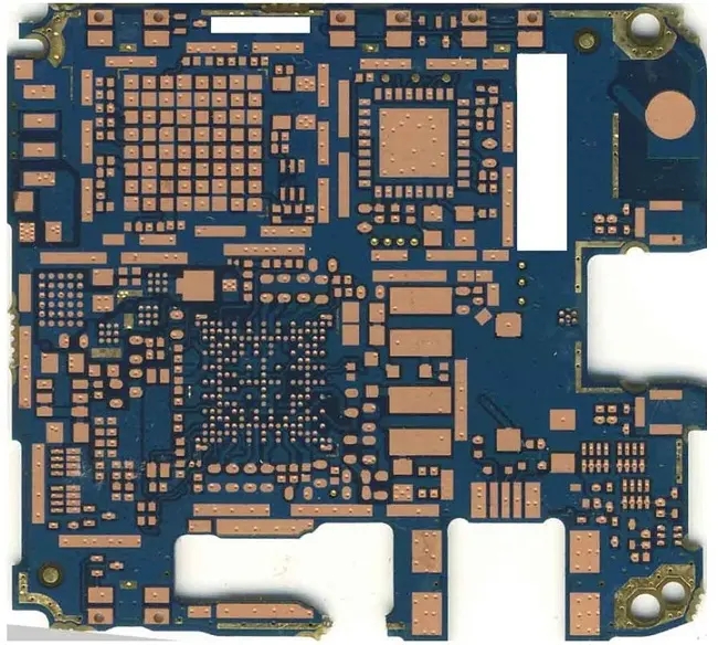
Pcb through hole plating and copper plating
In the production of circuit boards in the electronic industry, lead solder has always been the user of circuit board welding. In the past decades, this technology has been widely used in countless assembly and packaging products, and all circuit boards can adapt to this mature welding technology. Various quality and reliability standards, testing methods and management processes are all based on this lead welding technology.
The ban on lead led by ROHS (European Union Directive on Restricting the Use of Hazardous Substances) has had a great impact on the board and process of the whole circuit board, with the main focus on the change of welding technology. In addition to welding technology, the impact caused by this limitation also involves the change of PCB materials. In other words, even if the PCB material does not contain lead, it does not mean that it is compatible with lead-free technology. The so-called SAC305 alloy (tin, silver, copper) has been preferred in the new welding, and its melting point is about 34 ℃ higher than the current tin lead eutectic solder. The current task is how to use this lead-free solder to achieve the welding performance of the old lead alloys. In order to keep up with the latest development of PCB in sheet metal, reflow and flux, the operators must invest a lot of manpower and material resources to avoid falling in the transformation.
1、 Glue removal slag and plating through hole
(1) , circuit board glue removal residue
When the circuit board adopts the green process, it will bring many impacts to the current processes such as glue removal and through-hole plating. The current connotation of the so-called green process is as follows:
◆ Halogen free substrate ◆ Lead free welding resistant substrate ◆ Cyanide free chemical copper process
◆ Chemical copper process without E D TA ◆ Chemical copper process without formaldehyde
Halogen free plates refer to those that do not contain odorant flame retardants. When the adhesive residue or PTH process is carried out, many incompatibilities will inevitably occur. At this time, the cooperation of circuit board substrate manufacturers is also needed to develop new flame retardant and additive plates that can match the later process. The downstream process of these new components must be re evaluated to find out the best working conditions. In this way, process suppliers and circuit board manufacturers will inevitably increase a lot of work. Another important challenge is that green production will inevitably lead to premature aging and poisoning of some processes. For example, the filler (Fi11er) in the plate will shorten the active period of the de gelling solution, and may also affect the activation reaction of tin oxide before chemical copper. These irritations need to be evaluated and further studied.
As for the plates that can withstand lead-free welding, some halogen-free materials also have to face the question of whether they can adapt or not. How can they still have better performance after changing the composition of the base material, and how can they pass the strict test between T260 and T288 heat-resistant jasper? They need to continue to work hard to improve. Many new lead-free substrates on the market are almost all based on phenol (P N) instead of dicyandiamide (Dicy) as the hardener of epoxy resin, or other special resin mixtures. For lead-free and halogen-free materials, it is also very important to use fillers to reduce the number of swelling and improve the electrical properties. All new plates must be matched with potassium permanganate degumming slag, and the possible poisoning and sensitivity must be discussed in depth. AtoTech is carrying out such research work. For many traditional standard substrates, halogen-free substrates and lead-free substrates need to be discussed in depth. The following is part of the work.
◆ Standard formula and powerful permanganate degumming residue solution with three kinds of bulking agents
◆ The absorptivity of tin metal in the activation reaction before cuprization
◆ Coverage and adhesion of chemical copper process
◆ Pollution control of key tank liquid
Part of the results can clearly show the adaptability of each substrate and the demand for individual substrate evaluation.
(2) Chemical copper process without cyanide.
Cyanide has been used as stabilizer for a long time in the chemical copper process. Although the content of this cyanide in the chemical copper solution is very small, it is better to use less or not because of its high toxicity. Under the pressure of environmental protection, all new chemical copper supplied by liquid medicine manufacturers emphasize that it has no cyanide, and these new products are now used in horizontal and vertical processes.
(3) Chemical copper process without EDTA
EDTA is a chelating agent. NtYm is used in the industry and chemical copper manufacturing process. Because of its strong canthariding property, it will capture divalent metal ions into the tank solution and become wrong ions, so that it can be suspended in the solution. Therefore, in the process of wastewater treatment, lead or other metal ions to be precipitated will chelate with EDTA and cannot be precipitated, resulting in difficulties in wastewater treatment. Once the cantharides cannot be destroyed by wastewater treatment, heavy metals will be released into the environment and cause pollution.
In order to eliminate the harm of EDTA to the environment, the green process hopes to use other weaker canthariding agents, such as natural grape products, tartaric acid, as substitutes, so that it can be easily reprocessed and biodegraded. As early as the introduction of horizontal chemical copper, Atoll decided to use the tank solution of tartaric acid chemicals that is harmless to the environment; Since the first horizontal system was installed in 1899, the chemical copper system without EDTA has been continuously used. This trend has become the trend of all liquid medicine suppliers.
(4) Formaldehyde free chemical copper process
Formaldehyde has recently been proved to be a carcinogenic substance, which has been upgraded from a possible carcinogen to a truly carcinogenic substance. The newly published standards for harmful substances mean that the industry should seek alternatives to formaldehyde as soon as possible. At present, there are many liquid medicines on the market that advertise direct electroplating without formaldehyde. Therefore, the improved chemical copper has become an urgent process to find the solution. At present, one or two kinds of improved chemical copper are in the small trial stage, and the latest generation of formaldehyde free system has been applied in the soft board manufacturing process. The trend of taking green circuit boards as the theme has had an impact on through hole processes such as glue removal slag and chemical copper. At present, the biggest impact is halogen-free and lead-free substrates. For the online use of such new plates, it is inevitable that the existing manufacturing process will be impacted. We must be careful to introduce them gradually, and it is better to establish a set of optimal practices to achieve the best results.
2、 Electroplated copper
It is better to control the thickness ratio of hole copper and face copper for electroplating copper. The pretreatment and copper plating should be adjusted for the new lead-free welding plate, such as the hole aspect ratio or the line width and spacing in the line copper plating. Electroplated copper coating must have good copper thickness uniformity and excellent mechanical properties, such as Elongation and Ductility, to withstand the test of subsequent multiple processes. Only in this way can the finished circuit board have enough reliability and meet the customer's quality standards. There is a new Thermal Cycling measurement technology that can accurately evaluate PCB quality. Compared with the production of traditional circuit boards, the so-called green PCB production is the use of lead-free soldering and its related new parameters, which will have a great impact on copper electroplating.
The differences between lead-free soldering and traditional soldering of circuit boards are as follows:
◆ The welding temperature is about 34 ℃ higher than that of those with lead.
◆ The high temperature in welding operation lasts for a long time.
Higher welding temperature and longer holding time cause the expansion of plate in Z direction to increase, and the tensile stress of electroplating copper layer in through-hole to increase. This increased tensile stress on the copper layer is very similar to the traditional measurement method of copper electroplating reliability. The general practice is to conduct thermal stress test on the test piece in the tin lead alloy at the specified temperature by using the tin floating or tin dipping method. In order to know the results quickly, the S T method of interconnect thermal stress has been adopted. It can be seen from various tests that the sequence of factors affecting the reliability of copper electroplating is as follows:
◆ Thermal expansion coefficient CTE of PCB substrate in Z direction.
◆ Plate thickness.
◆ Through hole diameter.
◆ Plating copper thickness.
PCB base material has the greatest influence on the current welding reliability, so it can be predicted that the influence on the lead-free welding reliability should also be the largest.
(1) Influence of lead-free soldering times on copper electroplating
There are a series of test methods for the influence of lead-free soldering of circuit boards on the reliability of electroplating copper. First, the (graphic) circuit copper plating is carried out on the vertical line production with direct current, and the copper thickness reaches 3 Oum. The following is the key description of the test board production:
◆ The thickness of the plate is 1.5 m m, and the aperture is 0.4 m m and 1.2 m m
◆ Six layer board including circuit copper plating
◆ Base material characteristics: Tg1: 131.1 ℃, Tg2: 137.8 ℃.
The plate used is the standard: low T g material of F R 4, which is expected to fail in the first stage of the reliability test. T g=6.6 ℃ indicates that the polymer of the base material may not be fully polymerized during the pressing process, so the possibility of plate bursting may occur in subsequent thermal processes.
After copper electroplating, the test piece cut from the test board shall be subjected to the thermal stress (T h e r m a l S t r e s) test for 6 times before and after the Solder Floating at 288 ℃ X 10 seconds, and then the microsection shall be performed. Other test pieces from the same source have been subjected to thermal stress test of process ST, and a total of four test welds have been performed according to the lead-free welding temperature curve of process P C standard, and then 6 times of 10 second 288 ℃ bleached tin thermal stress test each time, and finally they are compared and interpreted.


Just upload Gerber files, BOM files and design files, and the KINGFORD team will provide a complete quotation within 24h.