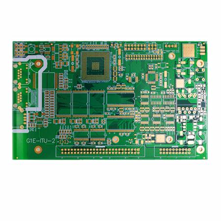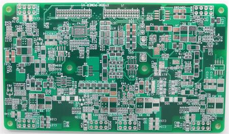
When the clock frequency exceeds 5MHz or the signal rise time is less than 5ns, in order to control the area of the signal loop well, it is generally necessary to use a multilayer board design (high-speed PCBs are generally designed with multilayer boards). When designing multilayer boards, we should pay attention to the following principles:

1. The key wiring layer (the layer where clock line, bus, interface signal line, radio frequency line, reset signal line, chip selection signal line and various control signal lines are located) should be adjacent to the complete ground plane, preferably between two ground planes, as shown in Figure 1. Key signal lines are generally strong radiation or extremely sensitive signal lines. Wiring close to the ground plane can reduce the area of its signal circuit, reduce its radiation intensity or improve its anti-interference capability.
2. The power supply plane shall be retracted relative to its adjacent ground plane (the recommended value is 5H~20H). Shrinking the power plane relative to its return ground plane can effectively suppress the "edge radiation" problem, as shown in Figure 2.
In addition, the main working power supply plane of the single board (the most widely used power supply plane) should be close to its ground plane to effectively reduce the loop area of the power supply current, as shown in Figure 3.
3. Whether there is no signal line ≥ 50MHz at the TOP and BOTTOM layers of the board. If so, it is better to walk the high-frequency signal between two plane layers to suppress its radiation to space.
Knowledge expansion: The number of layers of a multilayer board depends on the complexity of the circuit board. The number of layers and stacking scheme of a PCB design depend on such factors as hardware cost, outgoing lines of high-density components, signal quality control, schematic signal definition, PCB manufacturer's processing capability baseline, etc.
From the point of view of signal routing, a good PCB layering strategy should be to place all the signal routing on one or several layers, which are close to the power layer or the grounding layer. For power supply, a good layering strategy should be that the power layer is adjacent to the ground plane, and the distance between the power layer and the ground plane should be as small as possible. This is what we call "layering" strategy.
The excellent PCB layering strategies are as follows:
1. The projection plane of the wiring layer should be within the area of its return plane layer. If the PCB wiring layer is not within the projection area of its return plane layer, there will be signal lines outside the projection area during wiring, causing the "edge radiation" problem, and also increasing the area of the signal circuit, leading to increased differential mode radiation.
2. Try to avoid setting adjacent wiring layers. Because parallel signal routing on adjacent wiring layers will cause signal crosstalk, if it is impossible to avoid adjacent wiring layers, the layer spacing between the two wiring layers should be appropriately increased to reduce the layer spacing between the wiring layers and their signal loops.
3. The projection planes of adjacent plane layers shall not overlap. Because when the projection overlaps, the coupling capacitance between layers will cause the noise between layers to be coupled.


