
Professional PCB manufacturing and assembly
Building 6, Zone 3, Yuekang Road,Bao'an District, Shenzhen, China
+86-13410863085Mon.-Sat.08:00-20:00

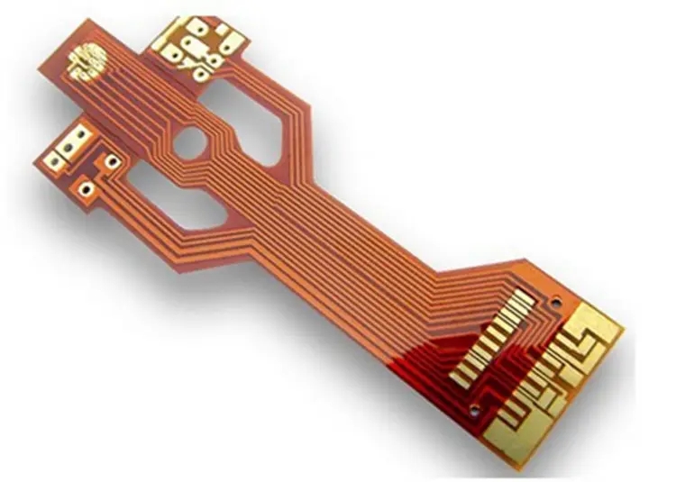
In recent years, flexible circuit board (FPC) has become one of the fastest growing sub industries in the printed circuit board industry.
Operation steps of flexible circuit board welding method:

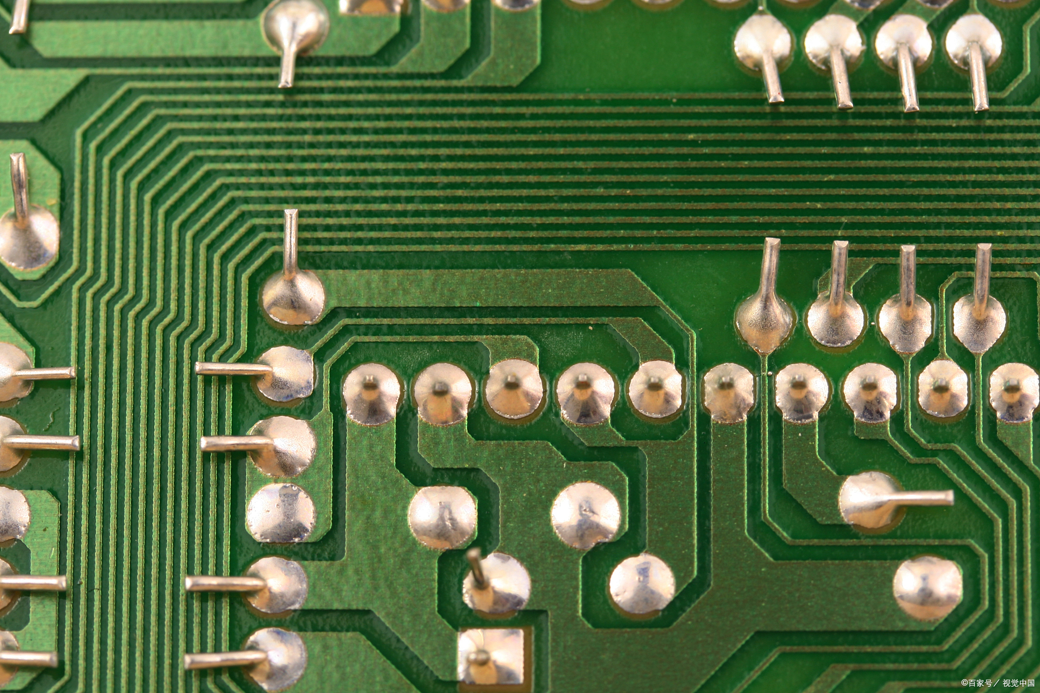
1. Before welding, apply flux on the bonding pad and treat it with a soldering iron once to avoid poor tin plating or oxidation of the bonding pad, which may lead to poor soldering. Generally, the chip does not need to be treated.
2. Carefully place PQFP chip on PCB board with tweezers, and be careful not to damage pins. Align it with the bonding pad, and ensure that the chip is placed in the correct direction. Adjust the temperature of the soldering iron to more than 300 ℃, dip a small amount of solder on the tip of the soldering iron, press the chip in the aligned position down with a tool, add a small amount of flux on the pins at the two diagonal positions, still press the chip down, solder the pins at the two diagonal positions, so that the core is fixed but cannot be moved. Recheck the alignment of the chip after welding the diagonals. If necessary, it can be adjusted or removed and re aligned on the PCB.
3. When welding all pins, solder should be added to the tip of the soldering iron, and all pins should be coated with flux to keep the pins wet. Contact the end of each pin of the chip with a soldering iron tip until you see solder flowing into the pin. During welding, keep the tip of the soldering iron parallel to the pin to be welded to prevent overlapping due to excessive soldering tin.
4. After welding all pins, soak all pins with flux to clean solder. Remove excess solder where needed to eliminate any shorts and laps. Finally, use tweezers to check whether there is faulty soldering. After the inspection, remove the flux from the circuit board and carefully wipe the hard brush along the pin direction with alcohol until the flux disappears.
5. The chip resistance capacitance component is relatively easy to solder. You can first put tin on a solder joint, then put one end of the component, clamp the component with tweezers, and then check whether it is placed correctly after welding one end; If it is aligned, weld the other end.
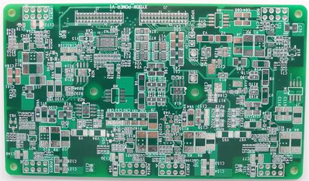
In the layout, when the size of the circuit board is too large, although the welding is easier to control, the printing line is long, the impedance increases, the noise resistance decreases, and the cost increases; If it is too small, the heat dissipation will drop, the welding is not easy to control, and the adjacent lines will easily interfere with each other, such as the electromagnetic interference of the circuit board. Therefore, PCB design must be optimized:
(1) Shorten the connection between high-frequency components and reduce EMI interference.
(2) Components with large weight (such as more than 20g) shall be fixed with supports and then welded.
(3) Heat dissipation shall be considered for heating elements to prevent large Δ In case of defects and rework, the thermal sensor shall be far away from the heat source.
(4) The arrangement of elements shall be as parallel as possible, which is not only beautiful but also easy to weld, and it is suitable for mass production. The circuit board is designed as a 4:3 rectangle (preferred). The wire width shall not be abrupt to avoid the discontinuity of wiring. When the circuit board is heated for a long time, the copper foil is easy to expand and fall off. Therefore, large area copper foil should be avoided.


Just upload Gerber files, BOM files and design files, and the KINGFORD team will provide a complete quotation within 24h.