
Professional PCB manufacturing and assembly
Building 6, Zone 3, Yuekang Road,Bao'an District, Shenzhen, China
+86-13410863085Mon.-Sat.08:00-20:00

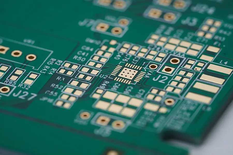
A fast signal does not travel only along a visible copper trace. Its return current also needs a continuous low-impedance path on a nearby reference plane. When that path is interrupted, the current must take a longer route, the loop area increases, and the PCB becomes more likely to suffer from noise, crosstalk and electromagnetic interference.
The following eight checks can be used during PCB layout review before Gerber files are released.
1. Keep a continuous reference plane below high-speed traces
Route high-speed signals over an uninterrupted ground plane whenever possible. Avoid crossing plane splits, voids or large clearance areas. A continuous reference plane gives return current a short path directly below the signal trace and helps control impedance.
2. Do not route critical signals across split power planes
A trace that crosses a split forces its return current to travel around the gap. This increases loop area and can create radiation and coupling problems. If a crossing cannot be avoided, review the stackup and provide an appropriate return path close to the transition.
3. Add nearby stitching vias when changing layers
When a signal moves from one layer to another, its return current may also need to move between reference planes. Place ground stitching vias close to the signal via so the return current does not need to search for a distant connection.
4. Review connector return paths
High-speed interfaces should have enough ground pins near signal pins. Check that the connector footprint, cable pinout and board stackup maintain a continuous return path from one board or cable section to the next.
5. Keep decoupling loops short
Place decoupling capacitors close to the power pins they support. Use short, wide connections and nearby vias to the power and ground planes. A small current loop improves the capacitor's effectiveness at high frequency.
6. Control gaps around crystals and clocks
Clock and crystal circuits switch quickly and can become strong noise sources. Keep their traces short, avoid routing unrelated signals through the area, and maintain a clear reference plane below the circuit unless the component manufacturer's layout guidance specifies otherwise.
7. Check differential pairs together with their reference plane
Pair spacing and length matching matter, but the reference plane also matters. Keep both traces on the same layer, maintain consistent geometry, and avoid routing the pair across plane discontinuities. Reduce unnecessary vias and keep the transition structure symmetrical.
8. Inspect the return path during the final DRC review
Traditional design rule checks find width, clearance and connectivity errors, but they may not reveal a poor return-current path. During the final review, inspect clocks, high-speed buses, switching power circuits and connector transitions manually. Confirm that every critical signal has a nearby and continuous reference.
Practical pre-release checklist
- Critical traces stay over a continuous reference plane
- No high-speed trace crosses a plane split or large void
- Layer transitions have nearby ground stitching vias
- Connectors provide adjacent ground returns
- Decoupling capacitor loops are short and direct
- Clock and crystal routing follows device guidance
- Differential pairs maintain consistent geometry and reference
- Gerber and drill outputs match the reviewed stackup
Return-path review should be completed together with impedance, spacing, stackup and manufacturability checks. Kingford provides PCB layout and design services as well as PCB manufacturing services for prototype and production projects.



Just upload Gerber files, BOM files and design files, and the KINGFORD team will provide a complete quotation within 24h.