
Professional PCB manufacturing and assembly
Building 6, Zone 3, Yuekang Road,Bao'an District, Shenzhen, China
+86-13410863085Mon.-Sat.08:00-20:00

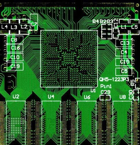
PCBis a printed circuit board, which is the carrier of electronic circuits. In modern electronic products, PCB is almost used. In many pcb manufacturing enterprises, PCB design is the last link of circuit design, and it is also a redesign of the principle circuit. Some new engineers tend to underestimate the importance of PCB design and leave this tedious and laborious work to technicians to complete. Here I will tell a story about PCB design first.

Compared with the early dial-type electronic telephones, it adds a dual tone/pulse dial control integrated circuit to the circuit, and some products also add hands-free Call function, when users use the phone, if they press the hands-free button, they can answer or speak out without picking up the phone. Anyone who is familiar with the principle of the telephone circuit knows that the hands-free circuit is composed of an "automatic receiving/transmitting control circuit" and an "audio power amplifier circuit". These circuits are implemented by ready-made dedicated ICs, and there is no need for innovative design in principle. .
The phone's marketing plan, so the accident was delayed for years. It was later found out that the reason for the false trigger of the hands-free was the poor design of the circuit's PCB. Later, the company's phone products, the hands-free buttons were all required to be changed to mechanical buttons, so that the telecom network access license was obtained. The direct economic loss caused by this incident to PCB manufacturing enterprises is as high as tens of millions of yuan.
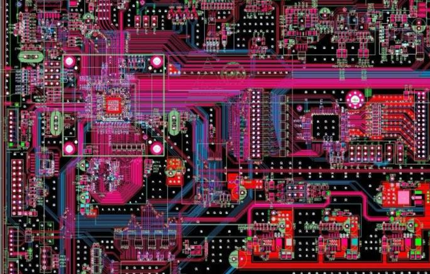
Some designers think that PCB design is a simple labor, which can be done by using PROTEL or other software tools through automatic layout and automatic routing. If a single panel cannot be routed, use a double-sided panel, if not, use a multi-layer panel, or set up jumpers. If the short jumper is not enough, use a long jumper. If it fails, use a jumper.
And I know an old engineer who didn't use a computer when they designed the PCB in the early years, but they can still complete the circuit PCB design containing hundreds of thousands of components. Moreover, the PCB layout and wiring they designed are quite neat, with very few jumpers and jumpers, and the original devices are arranged neatly and reasonably, and meet the requirements of the process specification. The early domestic black and white TV PCBs we saw belonged to the masterpieces of engineers of their era.
Although I used a computer for a long time when I designed the PCB. But I still feel that these old engineers must have some tricks to learn from in PCB design. It is difficult for our young engineers to imagine how they used pencils and graph paper to complete complex PCB designs. Indeed, I also gained a lot of experience from him, such as: how to arrange components so that they can be easily routed, how to effectively use the board space under the dual in-line IC, and how to plan the layout as much as possible before wiring and many more.
My own experience is: PCB design is not only technology, but also art. Art involves a lot of subjective factors, so engineers should also pay attention to improving their self-cultivation.
Tools help us do a lot of the tedious work, but what it does automatically isn't ideal for every product. Because what it helps us complete is the common and general aspect of product design, not the optimal design of the product automatically. The connection method, in a sense, only connects the devices to be connected together. Therefore, to really design the pcb of a product, it is more that the designer analyzes the situation of the product specifically, so as to complete a very unique design.


Just upload Gerber files, BOM files and design files, and the KINGFORD team will provide a complete quotation within 24h.