
Professional PCB manufacturing and assembly
Building 6, Zone 3, Yuekang Road,Bao'an District, Shenzhen, China
+86-13410863085Mon.-Sat.08:00-20:00


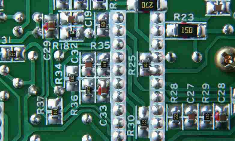
The goal of PCB design is to be smaller, faster and less costly. Since the interconnect point is the weakest link on the circuit chain, in RF design, the electromagnetic properties at the interconnect point are the main problem facing the engineering design, and each interconnect point should be investigated and the existing problems should be solved. The interconnection of the circuit board system includes three types of interconnection: chip to circuit board, PCB intra-board interconnection and signal input/output between PCB and external devices. This article mainly introduces the PCB board interconnect for high-frequency PCB design practical skills summary, I believe that through understanding this article will bring convenience to the future PCB design.

PCB design chip and PCB interconnection is important for design, but the main problem of chip and PCB interconnection is that the basic structure of PCB material will become a factor limiting the growth of interconnection density. This article shares practical tips for high frequency PCB design.
As far as high-frequency applications are concerned, PCB in-board interconnect for high-frequency PCB design techniques are:
1, the transmission line corner to use 45° Angle to reduce the loss;
2, to use insulation constant value strictly controlled by the level of high-performance insulated circuit board. This method is conducive to the effective management of the electromagnetic field between the insulation material and the adjacent wiring.
3, to improve the PCB design specifications for high-precision etching. Consider specifying a total error of line width of +/-0.0007 inches, managing undercut and undercut of a cabling shape, and specifying cabling side wall plating conditions. Overall management of the wiring (wire) geometry and coating surfaces is important to address the skin effects associated with microwave frequencies and to achieve these specifications.
4. Tap inductance exists in the prominent lead, and components with leads should be avoided. In high frequency environments, surface mounted components are preferred.
5, for the signal through the hole, to avoid the use of the sensitive plate through the hole processing (pth) process, because the process will cause the lead inductance at the hole. If a single hole on a 20-layer board is used to connect layers 1 to 3, the lead inductance can affect layers 4 to 19.
6, to provide rich ground. Moulded holes are used to connect the ground layers to prevent the effects of 3D electromagnetic fields on the circuit board.
7, to choose non-electrolytic nickel plating or dipping gold-plating process, do not use HASL method for electroplating. This electroplated surface provides a better skin effect for high frequency currents. In addition, this highly weldable coating requires fewer leads, helping to reduce environmental pollution.
8, solder resistance layer can prevent the flow of solder paste. However, due to the uncertainty of thickness and the unknown insulation properties, the entire surface of the plate covered with solder resistance material will lead to a large change in the electromagnetic energy in the microstrip design. Generally, welding dam (solderdam) is used as the welding resistance layer.
The above is for everyone to share the PCB board interconnect high frequency PCB design skills, if you are familiar with these methods, you can understand the use of back copper-covered coplanar microstrip design than strip line design is more economical and practical.
"Made in China 2025" focuses on innovation drive and transformation and upgrading, and the core and key of innovation lies in people. Technical talents are particularly critical in the electronic manufacturing industry. 2015HKPCA&IPCShow is not only committed to providing a display platform for product, technology and market information, but also strives to create a good opportunity to integrate domestic and foreign circuit board, electronic assembly and terminal electronic manufacturing customers for technical exchange and gather talents.
A number of colorful educational conferences were held during the exhibition. Every year, the show invites heavyweight speakers to share a series of the hottest and most practical technical issues or the latest market trends. This year is no exception, according to the organizers of the exhibition, a number of highly influential industry leaders will attend the education event, the detailed list of please look forward to.
The previous popular industry exchange activities will continue to be held, such as the industry exchange, exhibitors and participants will show the latest research and development products and share the latest market information; Welcome dinner and golf tournament, allowing participants to better network in a relaxed environment; It has held five consecutive and well-received manual welding competitions, showing the superb skills of professionals.
The world's leading trading platform helps enhance market competitiveness
According to the Schanp Consulting Industry Analysis * report, in the past decade, the global PCB industry has continued to migrate to Asia, especially mainland China, and mainland China has quickly become a major producer of electronic products and PCB. Due to the potential of domestic market and manufacturing advantages, China has attracted foreign investment, and China has developed into the world's largest PCB production country. How to take advantage of the development opportunity of "Made in China 2025" has become a problem that every PCB or electronic assembly company must think about.


Just upload Gerber files, BOM files and design files, and the KINGFORD team will provide a complete quotation within 24h.