
Professional PCB manufacturing and assembly
Building 6, Zone 3, Yuekang Road,Bao'an District, Shenzhen, China
+86-13410863085Mon.-Sat.08:00-20:00

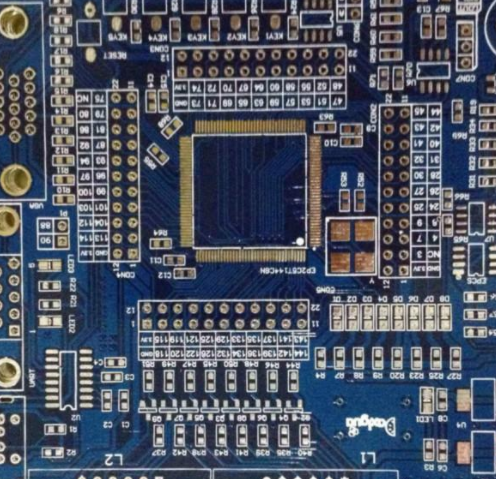

What problems should be paid attention to in high-speed PCB via design?
PCB vias are mainly composed of holes, pad areas around holes, and POWER layer isolation areas. In high-speed PCB design, multilayer PCB is often required, and via is an important factor in multilayer PCB design. In high-speed PCB multilayer boards, signals transmitted from one layer of interconnects to another layer of interconnects need to be connected through vias. Then, what problems should be paid attention to in high-speed PCB via design?
High speed PCB via design
1. Select a reasonable through hole size. For multilayer PCB design with general density, the ideal through-hole sizes for drilling, pad and POWER isolation area are 0.25mm, 0.51mm and 0.91mm; For some high-density PCBs, 0.20mm, 0.46mm and 0.86mm vias can also be used, or non through holes can be used; For the via of power supply or ground wire, consider using a larger size to reduce the impedance.
2. The larger the POWER isolation area, the better.
3. The signal wiring on PCB shall not change layers as much as possible, that is, through holes shall be minimized.
4. The use of thinner PCBs is conducive to reducing the two parasitic parameters of vias.
5. The pins of power supply and ground shall be close to the via, and the lead between the via and pin shall be as short as possible; At the same time, the power and ground leads should be as thick as possible to reduce impedance;
6. Place some grounding vias near the vias of signal layer change to provide short distance circuit for signals.
7. The length of vias is also the main factor affecting the inductance of vias. In high-speed PCB design, to reduce the problems caused by via, the via length is generally controlled within 2.0mm. For vias with a length greater than 2.0 mm, the impedance continuity of the vias can be improved to some extent by increasing the aperture of the vias. When the through-hole length is 1.0 mm or less, the optimal through-hole diameter is 0.20 mm~0.30 mm.
The above is the explanation given by the editor of pcb circuit board company. If you want to know more about PCBA, you can go to our company's home page to learn about it. In addition, our company also sells various circuit boards,
High frequency circuit board and SMT chip are waiting for your presence again.
Digital Image in PCB Design and Manufacturing
Oct 22,2022


Just upload Gerber files, BOM files and design files, and the KINGFORD team will provide a complete quotation within 24h.