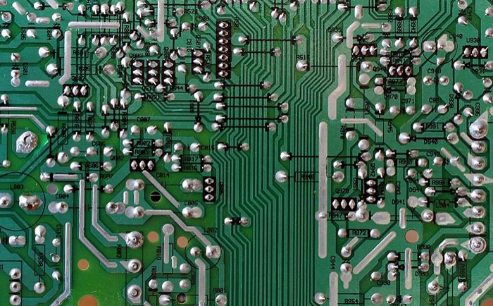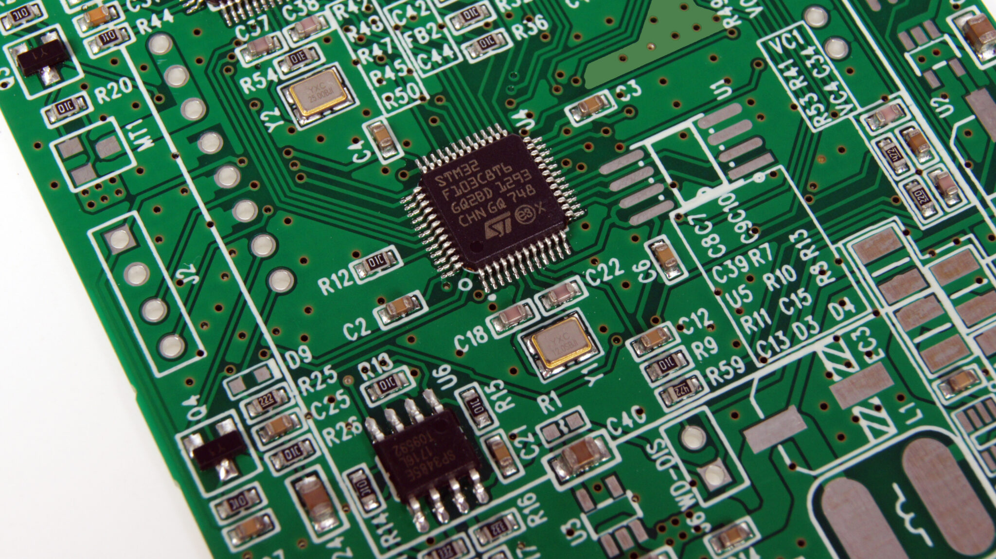
General principles of PCB component wiring
The general principles that designers need to follow during board layout are as follows.
(1) The principle of setting the spacing of printed traces of components. Spacing constraints between different nets are determined by factors such as electrical isolation, fabrication process, and component size. For example, if the pin spacing of a chip component is 8mil, the [Clearance Constraint] of the chip cannot be set to 10mil, and the designer needs to set a 6mil design rule for the chip separately. At the same time, the setting of the spacing should also take into account the production capacity of the manufacturer.
In addition, an important factor affecting components is electrical insulation. If the potential difference between two components or networks is large, electrical insulation needs to be considered. The gap safety voltage in the general environment is 200V/mm, which is 5.08V/mil. Therefore, when there are both high-voltage circuits and low-voltage circuits on the same circuit board, it is necessary to pay special attention to sufficient safety distances.
(2) Selection of line corner routing form. In order to make the circuit board easy to manufacture and beautiful, it is necessary to set the corner mode of the circuit during design, and you can choose 45°, 90° and arc. Generally do not use sharp corners, it is better to use arc transition or 45° transition, and avoid 90° or sharper corner transition.

The connection between the wire and the pad should also be as smooth as possible to avoid small sharp feet, which can be solved by filling teardrops. When the center distance between the pads is less than the outer diameter D of a pad, the width of the wire can be the same as the diameter of the pad; if the center distance between the pads is greater than D, the width of the wire should not be greater than that of the pad diameter.
When the wire passes between the two pads without being connected to it, it should maintain the largest and equal distance from them, and the distance between the wire and the wire should also be uniform and equal to the maximum.
(3) The method of determining the width of the printed trace. The trace width is determined by factors such as the current level and anti-interference flowing through the wire. The larger the current flowing, the wider the trace should be. Generally, the power line should be wider than the signal line. In order to ensure the stability of the ground potential (which is less affected by the change of the ground current), the ground wire should also be wider. Experiments have proved that: when the thickness of the copper film of the printed wire
When it is 0.05mm, the carrying capacity of the printed wire can be calculated according to 20A/mm2, that is, a wire with a thickness of 0.05mm and a width of 1mm can flow a current of 1A. Therefore, for general signal lines, a width of 10-30mil can meet the requirements; for high-voltage, high-current signal lines, the line width is greater than or equal to 40mil, and the spacing between lines is greater than 30mil. In order to ensure the anti-stripping strength and working reliability of the wire, within the allowable range of the board area and density, the wire should be as wide as possible to reduce the line impedance and improve the anti-interference performance.
For the width of the power line and the ground line, in order to ensure the stability of the waveform, try to make it as thick as possible if the wiring space of the circuit board allows. Generally, at least 50mil is required.
(4) Anti-interference and electromagnetic shielding of printed wires. The interference on the wires mainly includes the interference introduced between the wires, the interference introduced by the power line, and the crosstalk between the signal lines, etc. Reasonable arrangement and layout of the wiring and grounding methods can effectively reduce the interference source, so that the designed circuit board has more Good electromagnetic compatibility performance.
For high-frequency or other important signal lines, such as clock signal lines, on the one hand, the wiring should be as wide as possible; The wire "wraps" the signal wire, which is equivalent to adding a ground shield).
The analog and digital grounds should be wired separately and cannot be mixed. If it is necessary to unify the analog ground and the digital ground into one potential at the end, a one-point grounding method should usually be used, that is, only one point is selected to connect the analog ground and the digital ground to prevent ground loops from forming and causing ground potential shifts.
After the wiring is completed, a large area of grounding copper film, also known as copper coating, should be laid on the top and bottom layers where no wires are laid, to effectively reduce the impedance of the ground wire, thereby weakening the high-frequency signal in the ground wire, and at the same time The grounding of the area can suppress electromagnetic interference.
A via in the circuit board will bring a parasitic capacitance of about 10pF, which is especially harmful for high-speed circuits; at the same time, too many vias will also reduce the mechanical strength of the circuit board. Therefore, when wiring, the number of vias should be reduced as much as possible. In addition, when using penetrating vias (through holes), pads are usually used instead. This is because when the circuit board is made, some penetrating vias (through holes) may not be pierced due to processing, but the pads must be pierced during processing, which is equivalent to giving Production brings convenience.
The above are the general principles of PCB board layout and wiring, but in actual operation, the layout and wiring of components is still a very flexible job. The layout and connection methods of components are not unique, and the results of layout and wiring are very To a large extent, it still depends on the experience and thinking of the designer. It can be said that there is no standard to judge whether the layout and wiring scheme is right or wrong, only relative advantages and disadvantages can be compared. Therefore, the above layout and wiring principles are only used as a design reference, and practice is the only criterion for judging the pros and cons.
2.3 Special requirements for multilayer PCB board layout and wiring
Compared with simple single-layer boards and double-layer boards, the layout and wiring of multi-layer PCB boards have their own unique requirements.
For the layout of multi-layer PCB boards, in summary, it is necessary to reasonably arrange the layout of components using different power and ground types. The first purpose is to facilitate the division of the subsequent internal electrical layers, and at the same time, it can effectively improve the anti-interference ability between components.
The so-called reasonable arrangement of the layout of components using different power and ground types is to put the components that use the same power level and the same type of ground together as much as possible. For example, when there are multiple voltage levels such as +3.3V, +5V, −5V, +15V, −15V on the circuit schematic diagram, the designer should place components using the same voltage level in a certain area of the circuit board. Of course, this layout principle is not the only standard for the layout. At the same time, other layout principles (general principles of double-layer board layout) need to be taken into account. This requires designers to comprehensively consider various factors according to actual needs. Basically, try to put components that use the same power level and the same type of ground together. For the wiring of multi-layer PCB boards, it can be summed up in one point: take the signal line first, and then the power line. This is because the power and ground of multilayer boards are usually implemented by connecting the inner electrical layers. The advantage of this is that it can simplify the wiring of the signal layer, and effectively reduce the grounding impedance and the equivalent internal resistance of the power supply through the large-area copper film connection of the inner layer, and improve the anti-interference ability of the circuit; at the same time, the large-area The maximum current allowed by the copper film is also increased.
In general, designers need to arrange the layout of components using different power and ground types reasonably first, taking into account other layout principles, and then route the components according to the method introduced in the previous chapters (only signal lines), and divide them after completion. In the inner electrical layer, determine the network label of each part of the inner electrical layer, and finally connect through the vias and pads on the inner electrical layer and signal layer. When the pads and vias pass through the internal electrical layer, the pads or vias with the same network label will be connected to the internal electrical layer through some uncorroded copper films, and the copper film around the pads that do not belong to the network It will be completely corroded, that is to say, it will not conduct with the inner layer.


