
Professional PCB manufacturing and assembly
Building 6, Zone 3, Yuekang Road,Bao'an District, Shenzhen, China
+86-13410863085Mon.-Sat.08:00-20:00

PCB high current carrying method
three aspects:
1. PCB carrying large current operation method
2. Precautions for PCB carrying high current
3. Recommended operation for PCB carrying large current
1. PCB carrying large current operation method
Let me talk about three common high-current PCB design operation methods:
Increase the line width, usually 1A 1mm (40mil);
Copper thickness, 1oz, 2oz+++;
Open the window on the wire, add tin, silver, copper, etc.;
They are all basic exercises, so I won’t repeat them here.
2. Precautions for PCB carrying high current
First, there will be a very serious heating problem involved here, and even if the operation is carried out according to the above 1 and 2, the local heating phenomenon is difficult to deal with, because the current does not flow through the conductor evenly. Moreover, the resistivity of copper and tin is completely different, so the current often stays through the copper foil, and the heat of the plate will be very serious.
It should be known that the TG of commonly used FR4 is generally 140~170 degrees. Although it may not burn if it exceeds, it will directly lead to softening of the board and a serious decline in electrical performance.
Second, the reliability of the board will be greatly reduced, because of the practice of opening windows and adding tin to the wires, because the solder will melt in the event of a fault and cause an open circuit.
2. Recommended operation for PCB carrying large current
First, use copper bars, etc. as high-current conductors, or directly use copper plates to connect high-current parts.
Second, multi-layer boards are used for large current transmission, but thermal simulation is required, because the current does not flow evenly, which may cause local overheating, and specific analysis is performed according to the thickness and width of the copper clad board.
Third, the aluminum substrate, in comparison, the heat dissipation of the aluminum substrate is much better, and the pressure bearing capacity is also stronger, but it is still necessary to consider the temperature rise under the high current of 150A
The usual PCB design current will not exceed 10A, or even 5A. Especially in household and consumer electronics, usually the continuous working current on the PCB will not exceed 2A. But recently, we need to design power wiring for the company's products, and the continuous current can reach about 80A. Considering the instantaneous current and leaving a margin for the entire system, the continuous current of the power wiring should be able to withstand more than 100A. Then the question arises, what kind of PCB can withstand the current of 100A?
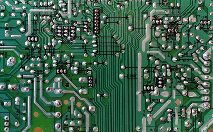
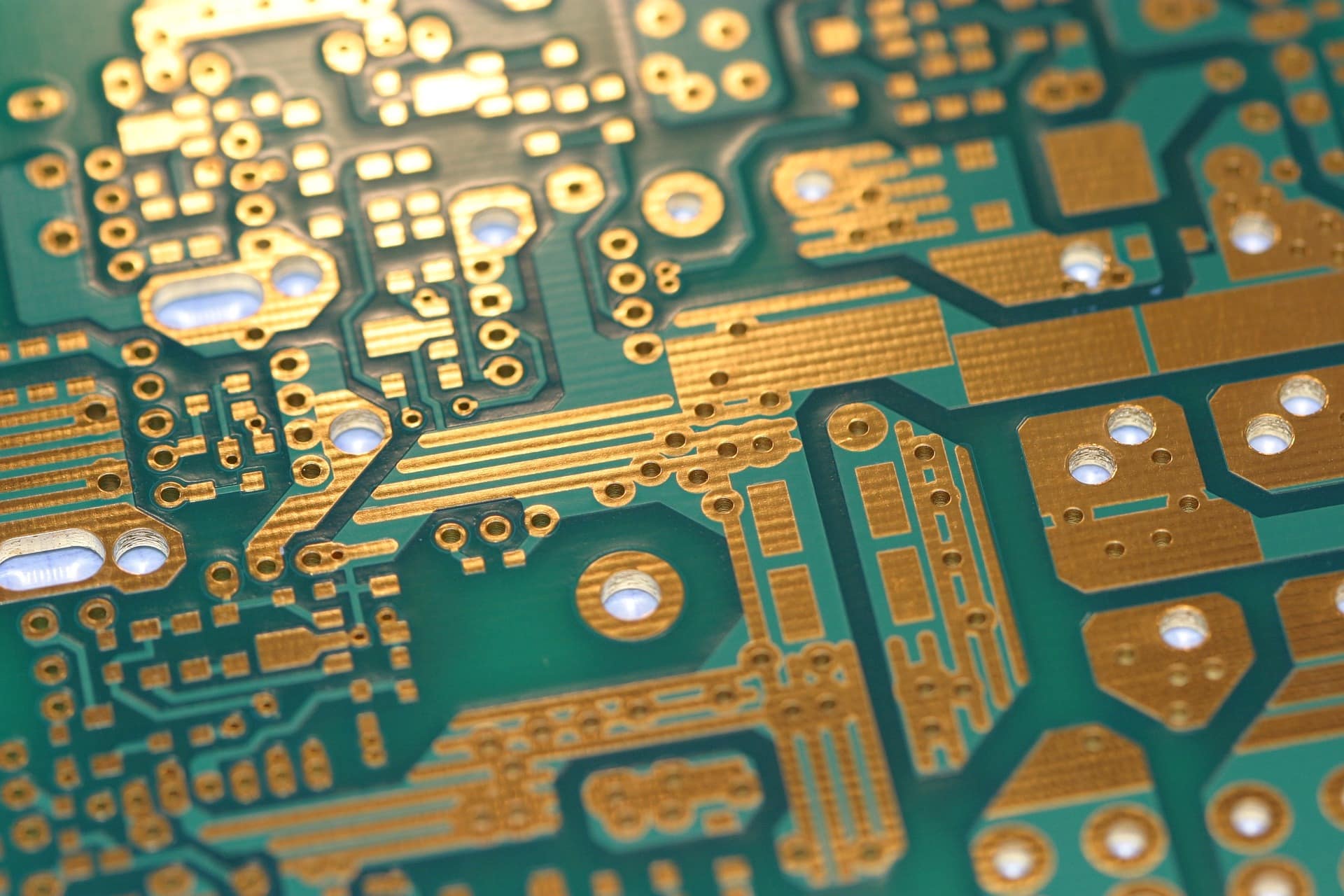
To find out the over-current capability of the PCB, we first start with the PCB structure. Taking a double-layer PCB as an example, this circuit board is usually a three-layer structure: copper skin, plate, and copper skin. The copper skin is also the path through which the current and signal in the PCB pass. According to middle school physics knowledge, we can know that the resistance of an object is related to material, cross-sectional area and length. Since our current is running on the copper skin, the resistivity is fixed. The cross-sectional area can be regarded as the thickness of the copper skin, which is the copper thickness in the PCB processing option. Usually the copper thickness is expressed in OZ, the copper thickness of 1OZ is converted to 35um, 2OZ is 70um, and so on. Then it can be easily concluded that when a large current needs to pass through the PCB, the wiring should be short and thick, and the thicker the copper thickness of the PCB, the better.
Actually, in engineering, there is no strict standard for the length of wiring. In engineering, three indicators are usually used: copper thickness/temperature rise/wire diameter to measure the current carrying capacity of the PCB board. The following two tables can be referred to:
From the table, it can be known that a circuit board with a copper thickness of 1Oz can pass a current of 4.5A through a wire with a width of 100mil (2.5mm) at a temperature rise of 10°. And as the width increases, the current-carrying capacity of the PCB does not increase strictly linearly, but the increase range gradually decreases, which is also consistent with the actual engineering situation. If the temperature rise is increased, the current carrying capacity of the wire can also be increased.
Through these two tables, the PCB layout experience that can be obtained is: increasing the copper thickness, widening the wire diameter, and improving the heat dissipation of the PCB can enhance the current carrying capacity of the PCB.
So if I want to carry a current of 100A, I can choose a copper thickness of 4Oz, set the trace width to 15mm, trace on both sides, and add a heat sink to reduce the temperature rise of the PCB and improve stability.
In addition to wiring on the PCB, you can also use binding posts to route the wiring.
Fix several binding posts capable of withstanding 100A on the PCB or on the product shell, such as surface mount nuts, PCB terminal blocks, copper posts, etc. Then connect the wires capable of withstanding 100A to the binding post by using terminals such as copper noses. In this way, large currents can go through the wires.
Even copper bars can be customized. It is a common practice in the industry to use copper bars to carry large currents. For example, transformers, server cabinets and other applications use copper bars to carry large currents.
Attached is the Bronze Medal Current Carrying Capacity Table:
In addition, there are some special PCB processes, and domestic manufacturers may not be able to find them. Infineon has a PCB that uses a 3-layer copper layer design. The top and bottom layers are signal wiring layers, and the middle layer is a copper layer with a thickness of 1.5mm, which is specially used for arranging power supplies. flow above 100A.
General principles of PCB component wiring
May 30,2023


Just upload Gerber files, BOM files and design files, and the KINGFORD team will provide a complete quotation within 24h.