
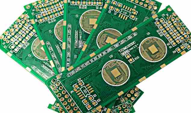
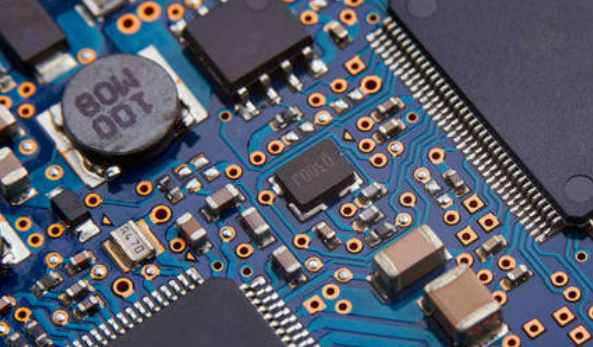
Professional PCB manufacturing and assembly
Building 6, Zone 3, Yuekang Road,Bao'an District, Shenzhen, China
+86-13410863085Mon.-Sat.08:00-20:00

Cause analysis of no copper in PCB hole sinking copper
Different resin systems and substrate materials are used, and different resin systems will lead to significant differences in the activation effect of copper sinking treatment and copper sinking treatment.
In particular, some CEM composite substrate and high-frequency plate silver substrate specificity, when doing chemical copper sedimentation treatment, need to take some special methods to deal with it, if the normal chemical copper sedimentation is sometimes difficult to achieve good results. Substrate pretreatment problems some substrate may absorb moisture and itself in the pressure synthetic substrate part of the resin curing is poor, so in the drilling may be because the strength of the resin itself is not enough to cause the drilling quality is very poor, drilling dirt or hole wall resin tear serious, so the material must be baked. In addition, some multilayer laminates may also appear poor curing of pp semi-cured sheet substrate area, which will directly affect drilling and removal of rubber slag activation of copper sedimentation.
The condition of drilling is too poor. The main performance is: resin dust in the hole, rough hole wall, serious burr in the hole, burr in the hole, copper foil nail in the inner layer, uneven length of torn section in the glass fiber area, etc., which will cause certain quality hazards to the chemical copper. Brush board in addition to mechanical methods to deal with substrate surface pollution and remove orifice burr/tip, surface cleaning, in many cases, but also to clean the hole dust. In particular, it is more important to deal with double panels without removing glue slag.

There is also one point to explain, we should not think that with the removal of glue slag can go out of the hole glue slag and dust, in fact, in many cases, the removal of glue slag process on the dust treatment effect is very limited, because the dust in the tank will form small micelles, so that the tank is difficult to deal with, the micelles adsorbed on the hole wall may form a hole plating tumor, It is also possible to fall off from the hole wall in the subsequent processing process, which may also cause the hole in the spot of no copper, so for multi-layer and double panels, the necessary mechanical brush plate and high pressure cleaning is also necessary, especially facing the development trend of the industry, small plate and high aspect ratio board is more and more common conditions.
Sometimes even ultrasonic cleaning to remove dust in the hole has become a trend. Reasonable and appropriate gel removal process can greatly increase the pore specific binding force and inner connection reliability, but the poor coordination between the gel removal process and the related tank will also bring some accidental problems. Insufficient removal of glue slag will cause micro-holes in the pore wall, poor combination of the inner layer, the pore wall separation, blowing holes and other quality hazards; Excessive gumming may also cause the glass fiber in the hole to protrude, rough in the hole, glass fiber cut-off point, copper infiltration, inner wedge hole broken inner layer of black copper separation caused by copper fracture or discontinuity or coating fold coating stress increase and other conditions.
In addition, the problem of coordination and control between several tanks is also very important. Insufficient bulk/swelling may result in insufficient gel removal slag; The puffing/swelling transition can be more able to remove the fluffy resin, then the copper will be activated badly when sinking copper, even if sinking copper may also appear after the process of resin sag, hole wall separation defects; For the gel removal tank, the new tank and the higher processing activity may also have some low degree of connection single-function resin double-function resin and part of the three-function resin excessive gel removal phenomenon, resulting in hole wall glass fiber prominent, glass fiber is difficult to activate and the chemical copper binding force is worse than between the resin, copper deposition after plating on the extremely uneven base, chemical copper stress will be multiplied, In severe cases, it can be obviously seen that after copper deposition, chemical copper pieces fall off from the hole wall, resulting in no copper in the subsequent holes.
Hole without copper open circuit, PCB industry is no stranger to people, but how to control? Many colleagues have asked many times. We made a lot of slices, but the problem still couldn't be completely improved. We always repeated it again and again. Today it was produced by this process, tomorrow it was produced by that process. In fact, it is not difficult to control, but some people can not adhere to the supervision and prevention of it, always the first, the last. The following is my personal opinion and control method of the hole without copper open circuit.
The reason for the absence of copper in the pore is nothing more than:
1. Drilling dust plug holes or holes thick.
2. There are bubbles in the solution when copper is sunk, and copper is not sunk in the hole.
3 hole line ink, no power on the protective layer, etching hole without copper.
4. After copper sinking or plate electric hole in the acid and alkali potion is not cleaned, parking time is too long, resulting in slow bite.
5. Improper operation, too long residence time in the process of micro-etching.
6. The punching plate pressure is too large, (the design punching is too close to the conductive hole) the middle is neatly disconnected.
7 electroplating potion (tin, nickel) penetration is poor.
In view of the seven causes of the problem of no copper in holes, the following improvements should be made:
1. Increase high pressure washing and glue slag removal processes for holes prone to dust generation (such as 0.3mm aperture below 0.3mm including 0.3mm).
2. Improve the activity and shock effect of the potion.
3. Change the printing screen and counterpoint film.
4. Extend the washing time and specify how many hours to complete the pattern transfer.
5. Set a timer.
6. Add explosion holes. Reduce the force on the board.
7. Do regular penetration tests.
The cleanliness of the board
Apr 20,2023


Just upload Gerber files, BOM files and design files, and the KINGFORD team will provide a complete quotation within 24h.