
Professional PCB manufacturing and assembly
Building 6, Zone 3, Yuekang Road,Bao'an District, Shenzhen, China
+86-13410863085Mon.-Sat.08:00-20:00

As we all know, when doing PCB design, ordinary PCB board as long as the precise design of mechanical size can be done. But if you encounter high frequency signals, the use of load line or long line, it is necessary to carry out special processing on these lines, otherwise, it is likely to cause reflection, cross-talk between lines and a series of signal interference problems. Therefore, when doing PCB design, especially when doing high-speed PCB design, we must do a good job of line signal imitation interference, shielding measures are very necessary.
Next, Shenzhen PCB design company -kingford will tell you how to do electromagnetic compatibility design of PCB design and wiring.
1. Appropriate wire width
Wire width is chosen to ensure both electrical performance and production convenience, usually by the minimum current value it can withstand. In order to reduce the electromagnetic interference impact caused by transient current on PCB board, it is necessary to control the line width in the design. Transient interference is usually caused by the inductance of a wire, which is directly proportional to the length of the wire and inversely proportional to the width of the wire. For signal lines that often have large transient currents, short and wide wires should be used, and if the layout space allows, a zigzi-shaped network should be used wherever possible.
2. Key points of component wiring
Component wiring design, mainly consider the following aspects:
One is the electrical performance; When wiring, we should try to put the devices more closely connected together. The layout of high-speed lines should be as short as possible. The power devices and small signal devices should be arranged separately.
Second, the location of the display; Whether the design is beautiful and neat, whether it is convenient for functional testing, later interface and connection use. In high-speed systems, the transmission delay of ground and interconnect lines is also the first design factor to be taken into account. The transmission time of signal transmission lines has a great impact on the total system speed of the circuit. If ordinary interconnect lines are used where high-speed lines are used, the delay time will be increased and the system speed will be greatly reduced.

3. Wiring rules for high frequency and high speed signals
Generally, equal wiring can reduce the inductance between wires, but in order to restrain the cross talk of PCB circuit wires, we should try to avoid long distance equal wiring in the design of wiring; The design of printed wire should avoid rapid turning, as far as possible to design into a uniform, with a certain curve; There are large current components on the circuit, as far as possible to separate ground wire, to avoid noise interference, small signal or sensitivity between the signal line grounding; High-speed signal adopts differential signal wiring design, so that the two difference lines in positive and negative pairs always keep coupling with each other on the transmission line, effectively reducing the electrical noise effect of the signal.
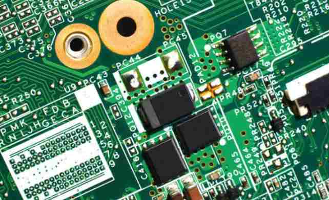
Shenzhen kingford has its own SMT plant, which can provide SMT SMT processing services of 0201 components with minimum package, supporting incoming material and sample processing and PCBA OEM. SMT components and plug-in components are the most commonly used components in SMT processing, and each has its own advantages and disadvantages.
SMT machining selection of SMT components advantages:
1. Reduce product volume: the volume of patch components is only about 1/10 of the traditional plug-in components; After SMT processing, the volume of electronic products is reduced by 40%~60%.
2. Improve production efficiency and reduce cost: SMT patch processing is easy to realize automation, improve production efficiency, save materials, energy, equipment, manpower, time, etc., and reduce cost by 30%~50%.
3. Light weight: the weight of the patch component is only 10% of that of the traditional plug-in component; Generally, after SMT is adopted, the product weight is reduced by 60%~80%.
4. High reliability and strong vibration resistance.
5. Good high-frequency characteristics, reduce electromagnetic and radio frequency interference.
6. Low defect rate of solder joint.
SMT machining selection of plug-in components advantages:
1. All are power type devices, which require high heat dissipation, and their performance is much higher than that of patch components, which can keep the performance of products stable and lasting.
2. Low failure rate, easy to test, can intuitively feedback out of bad, do not need to use special equipment.
3. Better anti-turbulence performance, in the face of high frequency, high amplitude vibration and turbulence, better than patch components to maintain the stability of the product.
Shenzhen kingford PCB design capability
Maximum signal design rate: 10Gbps CML differential signal;
Maximum number of PCB design layers: 40;
Minimum line width: 2.4mil;
Minimum line spacing: 2.4mil;
Minimum BGA PIN spacing: 0.4mm;
Minimum mechanical hole diameter: 6mil;
Minimum laser drilling diameter: 4mil;
Maximum number of pins:; 63000 +
Maximum number of components: 3600;
Maximum number of BGA: 48+.
PCB design service process
1. The customer provides schematic diagram to consult PCB design;
2. Evaluate quotation according to schematic diagram and customer design requirements;
3. The customer confirms the quotation, signs the contract and pays the project deposit;
4. Received advance payment and arranged engineer design;
5. After the design is completed, provide the screenshot of the document to the customer for confirmation;
6. The customer confirmed OK, settled the balance, and provided PCB design materials.


Just upload Gerber files, BOM files and design files, and the KINGFORD team will provide a complete quotation within 24h.