
Professional PCB manufacturing and assembly
Building 6, Zone 3, Yuekang Road,Bao'an District, Shenzhen, China
+86-13410863085Mon.-Sat.08:00-20:00

PCB design is a very detailed work, so the design should be very careful and patient, fully consider a variety of factors, including production and assembly processing, convenient maintenance and other issues. In addition, developing some good working habits in the design will make your design more reasonable, higher design efficiency, easier production and better performance. When good design is applied to everyday products, consumers will feel more assured and trusted. The basic PCB design process is as follows: preliminary preparation →PCB structure design → mesh guide → rule setting →PCB layout → Wiring → routing optimization and silk screen → network and DRC inspection and structure inspection → output light drawing → light drawing review →PCB board production/proofing data →PCB board factory engineering EQ confirmation → patch data output → project completion.
1, preliminary preparation this includes the preparation of the loading library and schematic diagram. In progress. Before PCB design, schematic SCH logic package and PCB package library should be prepared first. A wrapper library can be a wrapper library. PADS have their own libraries, but it is generally difficult to find suitable ones, and it is best to make their own packaging libraries based on the standard size data of the selected equipment. In principle, first do PCB packaging library, then do SCH logic packaging. PCB packaging library has high requirements, which directly affects the plate installation; SCH logic packaging requirements are more relaxed, as long as the definition of pin attributes and the corresponding relationship with PCB packaging. PS: Note the hidden pins in the standard library. Then the schematic design, ready to start. The PCB is designed.
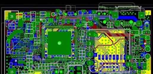
2, CB structure design This step according to the determined size of the circuit board and a variety of mechanical positioning, PCB drawing design environment PCB board surface, and according to the positioning requirements placed the required connectors, buttons/switches, screw holes, assembly holes, etc. And fully consider and determine the wiring area and non-wiring area (such as screw hole around the scope of non-wiring area). CB structure design
3. It is recommended to enter the plate frame before the mesh guide table. Import the board frame. Table 4. Rules Setting Reasonable rules for PCB design according to the specific situation. The rules we refer to are that the PADS restraint manager restricts the line width and safety spacing by restraining the manager at any link in the design process. The DRC test is marked using DRCMarkers. General rules are set before the layout, because sometimes some fanout work needs to be done during the layout, so the rules should be set before fanout, when the design project is larger, it can be more efficient to complete the design.
Note: The rules are set for better and faster completion of the design, in other words for the convenience of the designer. Common Settings include: Default line width/line distance
1. Ordinary signals.
2. Select and set the hole
3. Set the line width and color of important signals and power supplies.
4. Set the board layer.
5, PCB layout general layout according to the following principles: (1) according to the electrical performance reasonable partition, generally divided into: digital circuit area (fear of interference, fear of interference), analog circuit area (fear of interference), power driving area (interference source); (2) Circuits with the same function should be placed as close as possible, and each component should be adjusted to ensure the simplest connection; Adjust the relative positions of each functional block to make the connection between the functional blocks the simplest; (3) High quality components should consider the installation position and strength; The heating element should be placed separately from the temperature sensitive element, and the heat convection measures should be considered if necessary; (4) I/O driving device as close as possible to the edge of the printing plate, close to the outlet connector; (5) Clock generator (such as crystal oscillator or clock oscillator) should be as close as possible to the device using the clock; (6) Add a decoupling capacitor (usually a high frequency monolithic capacitor) between the power input pin of each integrated circuit and the ground; Tantalum capacitors can also be added around several integrated circuits when the board space is dense. (7) the relay coil should be added with discharge diode (1)N4148); (8) Layout requirements balance, density order, top-heavy or top-heavy PCB layout needs to pay special attention to, when placing components, must consider the actual size of components (area and height) and the relative position between components, in order to ensure the electrical performance of the circuit board and the feasibility and convenience of production and installation.
At the same time, on the premise of ensuring that the above principles can be reflected, modify the layout of the devices to make them neat and beautiful. The same devices should be placed neatly and in the same direction. This step is related to the overall image of the board and the difficulty of the next step wiring, so it needs to be strongly considered. Layout, can be uncertain of the place preliminary wiring, full consideration.
6, Wiring Wiring is the most important design process of the entire PCB. This has a direct impact on the design. PCB board performance is good or bad PCB in the design process, wiring generally has three levels: the first is the cloth, the most basic requirements of PCB design. If the line is not cloth through, flying line everywhere, it will be a substandard board, so to speak, has not started. Wiring two is to meet the electrical performance. This is a measure of whether the printed circuit board is up to scratch. This is done by carefully adjusting the wiring after wiring so that it achieves the best electrical performance. And then there's beauty. If your wiring is connected, there is nothing to affect the performance of the appliance, but at a glance it looks disorganized, colorful, colorful, and even if your appliance performs well, it will be garbage in the eyes of others. This brings great inconvenience to testing and maintenance. The wiring should be neat and uniform, not criss-cross. These should be achieved while ensuring the performance of electrical appliances and meeting other personal requirements, otherwise it is to neglect the essentials.

Wiring is mainly carried out according to the following principles: (1) In general, the power cord and ground wire should be wired first to ensure the electrical performance of the circuit board. Widen the width of the power supply and ground cable as much as possible, preferably wider than the width of the power cable. The relation between them is: ground > Power cord > Signal cable, usually signal cable width: 0.2 ~ 0.3mm (about 8-12mil), the minimum width can be up to 0.05 ~ 0.07mm (2-3mil), the power cable is generally 1.2 ~ 2.5mm (50-100mil). Digital circuit PCB wide ground wire can form a circuit that constitutes a ground network use (analog circuit ground cannot be used in this way).
(2) Advance wiring requirements of strict lines (such as high-frequency lines), input end and output end edge should avoid parallel adjacent to avoid reflection interference. If necessary, the ground line should be increased, the adjacent layer of wiring should be vertical, parallel easy to produce parasitic coupling.
(3) When the oscillator housing is grounded, the clock line should be as short as possible and cannot be attracted everywhere. Under the clock oscillation circuit, the area of the special high-speed logic circuit should be increased instead of other signal lines, so that the surrounding electric field is close to zero;
(4) as far as possible to use 45 ° as far as possible can not use 90 fold line to reduce the radiation of high frequency signal, fold line; (Double arcs are also required for high lines)
(5) Any signal line should not form a loop, if unavoidable, the loop should be as small as possible; The hole of the signal cable should be as small as possible. (6) The key line should be as short and thick as possible, and the protection ground should be added on both sides.
(7) When sensitive signals and noise field signals are transmitted through flat cables, the way of "ground - signal - ground" should be used.
(8) Test points should be reserved for key signals to facilitate production and maintenance testing
(9) After the schematic wiring is completed, the wiring should be optimized; At the same time, after the preliminary network inspection and preliminary network inspection, the ground wire of the unconnected area was filled with a large area of copper layer as the ground wire, and the unused place was connected to the printing plate as the ground wire. Or made of multilayer board, power supply, ground wire each account for a layer.
PCB wiring process requirements (can be set in the rules) (1) General signal wire width is 0.3mm(12mil), power cord width is 0.77mm(30mil) or 1.27mm(50mil); The distance between wire and wire and pad is greater than or equal to 0.33mm(13mil). In practical application, the distance should be considered to increase when conditions permit; When the wiring density is high, it is considered (but not recommended) that there be two wires between the IC pins with a line width of 0.254mm(10mil) and a line spacing of at least 0.254mm(10mil). In special cases, when the pin of the device is tight and the width is narrow, the width and distance between the wires can be reduced appropriately.
(2) Welding PAD (PAD) and transition hole (VIA) The basic requirements are: disk diameter greater than hole diameter 0.6mm; For example, universal pin resistors, capacitors, integrated circuits, etc., using disk/hole sizes of 1.6mm/0.8mm (63mil/32mil), sockets, pins, diode 1N4007, etc., using 1.8mm/1.0mm (71mil/39mil). In practical application, it should be determined according to the size of the actual components, and the size of the pad can be appropriately increased if conditions permit; The installation aperture of the components designed on the PCB board should be larger than the actual size of the component pins.2 ~ 0.4mm (8-16mil).
(3) Through hole (VIA) generally 1.27mm/0.7mm(50mil/28mil); When the connection density is high, the hole size can be appropriately reduced, but not too small, can consider using 1.0mm/0.6mm(40mil/24mil). (4) Pad, wire, hole spacing requirements PADandVIA: ≥0.3mm (12mil) PADandPAD: ≥0.3mm (12mil) PADandTRACK: ≥0.3mm (12mil) TRACKandTRACK: ≥0.3mm (12mil) High density: PADandVIA: ≥0.254mm (10mil) PADandPAD: ≥0.254mm (10mil) PADandTRACK: ≥0.254mm (10mil) TRACKandTRACK: ≥0.254mm (10mil) 7, wiring optimization and screen printing "no best, only better"! No matter how hard you try to design it and look at it after it's finished, there's still a lot you can change. A general design rule of thumb is that it takes twice as long to optimize your wiring as it does the first time. Feeling that there was no place to modify, then apply copper. Copper generally lay ground (pay attention to the separation of analog ground and digital ground), multilayer board may also need to lay power supply. For screen printing, be careful not to be blocked by equipment or removed by holes and pads. At the same time, design to face the surface of the element, the bottom text to do mirror processing, so as not to confuse the level.
8. It is generally necessary to check the network, DRC inspection and structure inspection before they are cleared. Every company will have its own CheckList, which covers the requirements of principle, design, production and other links. The following are the two main checking functions provided by the software. DRC check: Network, DRC check and structure check 9. Output optical drawing Before the output of optical drawing, ensure that the board is the latest version that has been completed and meets the design requirements. Optical drawing output files are used in plate factory, steel mesh factory, welding factory process files, etc. Output light drawing output files include (for example, four-layer board):
1) Wiring layer: refers to the conventional signal layer, mainly wiring. The names are L1,L2,L3,L4, where L stands for layer by layer. Wiring layer
2) Screen printing layer: refers to the level in the design document that provides information for processing screen printing. Usually, there is top screen printing and bottom screen printing when the top and bottom floors have equipment or signs. Naming: The top layer is named SILK_TOP; The underlying layer is named SILK_BOTTOM. Screen printing layer
3) Solder resistance layer: refers to the level of processing information provided for green coatings in the design document. Naming: The top layer is named SOLD_TOP; The bottom layer is named SOLD_BOTTOM. Solder shield
4) Steel mesh layer: refers to the level of processing information provided for solder paste coating in the design document, usually there are SMDS on the top and bottom layers. Under the condition of installation, there will be steel mesh top layer and steel mesh bottom layer. Naming: The top layer is PASTE_TOP; The bottom layer is called PASTE_BOTTOM.
5) The drilling layer (including two files, NCDRILL NC drilling file and DRILLDRAWING drilling Drawing) is named NCDRILL and DRILLDRAWING respectively.
10, light painting review after the output light painting to carry out light painting inspection, Cam350 open short circuit and other aspects of the inspection can be sent to the board factory board, later also pay attention to the board engineering and problem reply. 11. PCB board making data (Gerber light drawing data +PCB board making requirements + panel drawing)
12. PCB board factory project EQ confirmation (board making project and problem reply).
13. PCBA patch data output (steel mesh data, patch position number diagram, component coordinate file). Here's a project where all the workflow design of the PCB is done
Shenzhen kingford is a professional PCB design company engaged in electronic products layout layout design, mainly undertake multi-layer, high density PCB design and circuit board design proofing business. Proficient in the use of market mainstream PCB design software, professional and efficient communication to ensure the progress of PCB design, to help you seize the market opportunity one step earlier!


Just upload Gerber files, BOM files and design files, and the KINGFORD team will provide a complete quotation within 24h.