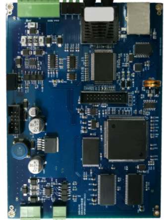
The laminated structure of PCB board is an important factor affecting its EMC performance and an important means to suppress electromagnetic interference. Before the design of multilayer PCB board, it is necessary to determine the PCB structure according to the size of the circuit, the size of the circuit board and electromagnetic compatibility (EMC) requirements. Shenzhen kingford PCB Design Company will introduce the six-layer PCB design laminated solution in accordance with EMC design.
The six-layer PCB design is in line with EMC design
In some six-layer PCB design schemes, the shielding effect of electromagnetic field is not good enough, and the effect of reducing the transient signal of the power busbar is very small. That kind of chip density larger, higher clock frequency design can consider six-layer PCB design.
The first layer scheme: sig-gndd-sig-pwr-gndd-sig;
This lamination solution results in better signal integrity. The signal layer is adjacent to the grounding layer, the power layer is paired with the grounding layer, the impedance of each routing layer can be well controlled, and the magnetic field lines can be well absorbed by both layers. In addition, a good return path can be provided for each signal layer when the power supply and formation are intact.
The second layer scheme: GND-SIG-GND-PWR-SIG-GND;
This lamination scheme is only applicable to the case where the device density is not very high. This lamination has all the advantages of the upper lamination, and the ground plane of the top and bottom layers is relatively complete, which can be used as a better shielding layer. It is important to note that the power layer should be near the layer that is not the main component plane, because the bottom plane will be more complete. Therefore, EMI performance is better than the first scheme.
For the six-layer PCB design, the spacing between the power layer and the formation should be minimized in order to obtain better power-ground coupling. Like 62mil plate thickness, although the layer spacing is reduced, it is not easy to control the distance between the main power supply and the formation is very small. Compared with the first scheme, the second scheme greatly increases the cost, so we generally choose the first scheme when stacking. In the design, to follow the 20H rules and mirror layer rules design.
2.PCB design impedance discontinuity solution

Everyone knows that PCB design impedance should be continuous. However, PCB designs will always have impedance discontinuity. What to do? The following Shenzhen kingford PCB design company for you to talk about the impedance can not be continuous solution.
What is characteristic impedance?
Characteristic impedance: Also known as "characteristic impedance", it is not DC resistance, belongs to the concept of long line transmission. In the high frequency range, a transient current will be generated between the signal line and the reference plane (power or ground plane) along the place where the signal arrives during signal transmission due to the establishment of an electric field.
If the transmission line is isotropic, there will always be a current I as long as the signal is being transmitted. However, if the output voltage of the signal is V, the transmission line will be equivalent to a resistance of size V/I in the process of signal transmission. This equivalent resistance is called the characteristic impedance Z of the transmission line.
In the process of transmission, if the characteristic impedance of the transmission path changes, the signal will reflect at the node where the impedance is discontinuous.
What factors affect characteristic impedance?
The factors affecting the characteristic impedance are: dielectric constant, dielectric thickness, wire width, copper foil thickness.
The solution of impedance discontinuity problem in PCB design
1. Gradient line
Some RF devices have small packaging, SMD pad width may be as small as 12mils, and RF signal line width may be more than 50mils, to use a gradient line, prohibited line width mutation.
Step 2: Corner
If the RF signal line is at a right Angle, the effective line width at the corner will increase, resulting in discontinuous impedance and signal reflection. To reduce discontinuity, there are two ways to treat corners: cut corners and round corners. The radius of the arc Angle should be large enough, generally speaking, to ensure that: R> 3W.
3. Large pad
When there is a large pad on the 50 euro fine strip line, the large pad is equivalent to the distributed capacitance, which destroys the characteristic impedance continuity of the microstrip line. Two methods can be taken at the same time to improve: first, the microstrip line medium thickened, and secondly, the ground plane below the pad is hollowed out, which can reduce the distributed capacitance of the pad.
4. Through the hole
The through hole is a metal cylinder plated in the through hole between the top and bottom of the circuit board. Signal holes connect transmission lines on different layers. The hole stump is the unused part of the hole. Through-hole pads are circular spacers that connect through-holes to top or internal transmission lines. Isolation panels are annular gaps within each power supply or ground to prevent short circuit to the power supply and ground.
5. Through-hole coaxial connector
Similar to the through-hole construction, the through-hole coaxial connector also has impedance discontinuity, so the solution is the same as the through-hole. The common methods to reduce the impedance discontinuity of through-hole coaxial connectors are as follows: using the disk-free process, appropriate outlet mode, and optimizing the diameter of the backplate.
Shenzhen kingford is a professional PCB design company engaged in electronic products layout layout design, mainly undertake multi-layer, high density PCB design and circuit board design proofing business. Proficient in the use of market mainstream PCB design software, professional and efficient communication to ensure the progress of PCB design, to help you seize the market opportunity one step earlier!


