
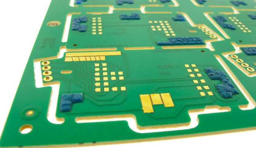
Professional PCB manufacturing and assembly
Building 6, Zone 3, Yuekang Road,Bao'an District, Shenzhen, China
+86-13410863085Mon.-Sat.08:00-20:00

1. Component layout
The layout is in accordance with the requirements of the electrical schematic diagram and the dimensions of the components, the components are evenly and neatly arranged on the PCB circuit board, and can meet the mechanical and electrical performance requirements of the whole machine. Whether the layout is reasonable or not not only affects the performance and reliability of PCB assembly parts and the whole machine, but also affects the difficulty of processing and maintenance of PCB and its assembly parts, so the layout should try to do the following:
The components are distributed evenly, and the components of the same unit circuit should be arranged relatively centrally to facilitate debugging and maintenance;
Connected components should be arranged relatively close to each other, in order to improve the wiring density and ensure the shortest distance;
For heat-sensitive components, the layout should be far away from the components with large heat;
Components that may have electromagnetic interference with each other shall be shielded or isolated.
2. Wiring rules
Wiring is to lay printed wires according to the electrical schematic diagram, wire table and required wire width and spacing. Wiring should generally comply with the following rules:
Under the premise of meeting the requirements of use, the order of selecting the wiring mode is single layer, double layer and multiple layer.
The wire layout between the two connecting disks should be as short as possible. Sensitive signals and small signals should go first to reduce the delay and interference of small signals. The input line of the analog circuit should be equipped with a ground wire shield; The wiring of the same layer should be evenly distributed; The conductive area on each layer should be relatively balanced to prevent the board from warping.
Signal line change direction should be oblique or smooth transition, and the radius of curvature is better to avoid electric field concentration, signal reflection and additional impedance.
The digital circuit and the analog circuit should be separated on the wiring to avoid interference with each other. If they are on the same layer, the ground wire system and the power system of the two circuits should be arranged separately. The signal lines of different frequencies should be separated by ground wires to avoid crosstalk. In order to test convenience, the design should set necessary breakpoints and test points.
When circuit components are grounded and connected to the power supply, the wiring should be as short as possible to reduce internal resistance.
The upper and lower cables should be perpendicular to each other to reduce coupling. Do not align or parallel the upper and lower cables.
Multiple I/O wires of high-speed circuits and I/O wires of differential amplifiers, balance amplifiers and other circuits should be equal in length to avoid unnecessary delay or phase shift.
When the welding pad is connected with a large conductive area, a fine wire with a length of not less than 0.5mm and a width of not less than 0.13mm should be used for thermal isolation.
The wire closest to the edge of the circuit board must be more than 5mm away from the edge of the printed board. If necessary, the ground wire can be close to the edge of the board. If a guide rail is to be inserted during the processing of a printed board, the distance between the wire and the edge of the board should be at least greater than the depth of the guide groove.
The public power cables and ground cables on the two panels should be placed close to the edge of the panel and distributed on the surface of the panel. The multilayer board can be arranged in the inner layer of the power layer and ground layer, through the metallized holes with each layer of the power line and ground wire, a large area of the inner layer of the wire, power line, ground wire should be designed into a network, can improve the bonding force between the layers of the multilayer board.
3. Wire width
The width of the printed wire is determined by the load current of the wire, the allowable temperature rise and the adhesion of the copper foil. Generally, the wire width of the printed board is not less than 0.2mm, and the thickness is more than 18μm. The finer the wire the more difficult it is to process, so in the wiring space allowed conditions, should be appropriate to choose some wide wire, the usual design principles are as follows:
Signal cables should have the same thickness, which is conducive to impedance matching. Generally, the line width is recommended to be 0.2~0.3mm (812mil). For power ground cables, the larger the line area, the better to reduce interference. It is best to shield the high frequency signal from the ground line, which can improve the transmission effect.
In the high-speed circuit and microwave circuit, the characteristic impedance of the transmission line is specified, and the width and thickness of the wire should meet the requirement of characteristic impedance.
In the design of high power circuit, the power supply density should also be considered. At this time, the line width, thickness and insulation performance between lines should be considered. If the inner conductor, the allowable current density is about half that of the outer conductor.
4, printed wire spacing
The insulation resistance between the wires on the surface of the printed board is determined by the distance between the wires, the length of the parallel section of the adjacent wires, and the insulating medium (including substrate and air). Under the condition of the wiring space, the distance between the wires should be increased appropriately.
5. Selection of components
The selection of components should fully take into account the actual area of PCB needs, as far as possible choose conventional components. Should not blindly pursue small size components, so as not to increase the cost, IC devices should pay attention to pin shape and foot spacing, less than 0.5mm foot spacing QFP should be carefully considered, it is better to directly choose BGA packaged devices. In addition, the packaging form of components, end electrode size, weldability, reliability of the device, temperature tolerance, such as can adapt to the needs of lead-free welding, should be taken into account.
After selecting the components, the components database must be established, including installation size, pin size and manufacturer's relevant information.
6. Selection of PCB substrate
The substrate should be selected according to the service conditions and mechanical and electrical performance requirements of PCB; According to the printed board structure to determine the number of copper-covered foil surface of the substrate (single, double or multilayer board); According to the size of the printed board, unit area bearing component quality, determine the thickness of the substrate board. The cost of different types of materials varies greatly, and the following factors should be considered when selecting PCB substrates:
Electrical performance requirements;
Tg, CTE, flatness and other factors as well as the ability of pore metallization;
Price factor.
7, printed board anti-electromagnetic interference design
The external electromagnetic interference can be solved by the shielding measures of the whole machine and the anti-interference design of the improved circuit. For the electromagnetic interference of PCB assembly itself, the following considerations should be taken into consideration when designing PCB layout and wiring:
Components that may affect or interfere with each other should be kept away from or shielded during layout.
For high frequency, high speed circuit, should try to design into double-sided and multilayer printed board. One side of the two panels is arranged with a signal line, and the other side can be designed as ground; The signal lines which are easy to be interfered can be arranged between the ground layer or the power layer in the multilayer board; For the strip line used in microwave circuit, the transmission signal line must be laid between the two layers, and the thickness of the dielectric layer between them should be calculated according to the need.
Transistor base printed line and high frequency signal line should be designed as short as possible to reduce the electromagnetic interference or radiation during signal transmission.
Components with different frequencies do not share the same ground cable. Ground cables and power cables with different frequencies should be arranged separately.
Digital and analog circuits do not share the same ground wire. There can be a common contact where the printed board connects to the external ground wire.
When the potential difference is relatively large components or printed lines, should increase the distance between each other.
8, PCB heat dissipation design
With the increase of the assembly density of components on the printed board, if the heat dissipation cannot be timely and effectively, the working parameters of the circuit will be affected, and even if the heat is too large, the components will fail. Therefore, the design of the heat dissipation of printed board must be seriously considered, and the following measures are generally taken:
Increase the copper foil area on the printed board and the ground surface of the high-power components;
Large heat components are not attached to the plate installation, or external radiator;
The inner ground wire of the multilayer plate should be designed into a network and close to the edge of the plate;
Choose a flame retardant or heat resistant type of sheet.
9. PCB should be made into arc Angle
PCB with right Angle is easy to get stuck when it is transmitted, so when designing PCB, it is necessary to do arc Angle treatment on the board frame, and determine the radius of arc Angle according to the size of PCB. Sectional board and PCB with auxiliary edge make circular Angle on auxiliary edge.

Thermal design requirements of PCBA
Feb 23,2023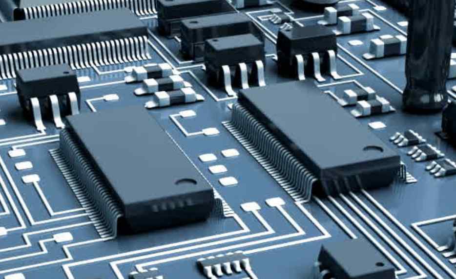


Just upload Gerber files, BOM files and design files, and the KINGFORD team will provide a complete quotation within 24h.