
Professional PCB manufacturing and assembly
Building 6, Zone 3, Yuekang Road,Bao'an District, Shenzhen, China
+86-13410863085Mon.-Sat.08:00-20:00

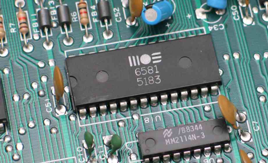
Width and spacing of printed wire are important design parameters, which affect not only the electrical performance and electromagnetic compatibility of PCB board, but also the manufacturability and reliability of PCB. The width of the printed wire is determined by the load current of the wire, the allowable temperature rise and the adhesion of the copper foil. The width and thickness of the wire determine the cross-sectional area of the wire, the larger the cross-sectional area of the wire, the larger the carrying capacity, but the current flowing through the wire will generate heat and cause the temperature of the wire to rise, the size of the temperature rise is affected by the current and heat dissipation conditions, and the allowable temperature rise is determined by the characteristics of the circuit, the operating temperature requirements of the components and the environmental requirements of the whole machine. So the temperature rise must be controlled within a certain range. Printed wire is attached to the insulating substrate, too high temperature will affect the adhesion of the wire to the substrate, so the width of the design wire should be considered in the selection of copper foil thickness on the basis of the substrate, the load current required by the wire, the temperature rise allowed by the wire and the adhesion of copper foil can meet the requirements to determine the width of the printed wire. For example, on copper foil with a wire width of no less than 0.2mm and a thickness of more than 35um, when the load current is 0.6A, the temperature rise will not exceed 10℃. Due to the SMT printed board and high density signal wire, the load current is very small, the wire width can reach 0.1mm, but the thinner the wire, the more difficult the processing, the smaller the load current capacity. So in the case of wiring space allowed, should be appropriate to choose some wide wire, general ground wire and power line should be designed wider, which is conducive to reducing the temperature rise of the wire, but also conducive to manufacturing.
The spacing of printed wires is determined by the insulation resistance, voltage resistance requirements and electromagnetic compatibility, as well as the characteristics of the substrate, and is also limited by the manufacturing process. The insulation resistance between the wires on the surface of the printed board is determined by the wire spacing, the length of the parallel section of the adjacent wire, the insulating medium (including the substrate and air), the processing quality of the printed board, temperature, humidity and surface pollution and other factors. Generally speaking, the higher the insulation resistance and resistance voltage requirements, the conductor spacing should be properly widened. When the load is larger, the distance between the wires is not conducive to heat dissipation, the temperature rise of the printed board with small wire spacing is also higher than that of the board with large wire spacing, so in the design, the load current of the larger wire and the adjacent wire with large potential difference, in the wiring space allowed, should be appropriately increased wire spacing, which is conducive to manufacturing, It is also helpful to reduce the mutual interference of high frequency signal lines. Generally, the width and spacing of ground cables and power cables are larger than that of signal cables. Considering the requirements of electromagnetic compatibility, the edge spacing of adjacent wires of high-speed signal transmission lines should not be less than twice the width of signal lines, which can greatly reduce the crosstalk of signal lines, and is also conducive to manufacturing.
When designing the printed circuit board, the appropriate width and distance should be selected according to the signal quality, current capacity and the processing capacity of the PCB manufacturer. At the same time, the following process reliability requirements should be considered:
1. According to the processing capacity of most PCB manufacturers, the line width/line distance is generally required to be no less than 4mil;
2. No right Angle turning point is allowed at the turning point of the wiring;
3. In order to avoid crosstalk between two signal wires, the distance between two wires should be separated when parallel cables are routed. It is best to adopt vertical crossover or add a ground wire between two signal wires.
4. Board wiring should be properly dense, when the density difference is too big should be filled with copper foil mesh;
5.SMT pad lead out of the wire, as far as possible vertical, avoid diagonal pull wire;
6. When the SMT pad is led from the pin width thinner than the wire, the wire cannot be covered from the pad, and should be led from the end of the pad.
7. When the leads of tightly spaced SMT pads need to be connected, they should be connected outside of the pads. Direct connection in the middle of the pads is not allowed.
8. As far as possible, crossing the wire between the welding pad of the fine-spaced components should be avoided. If it is necessary to cross the wire between the welding pad, it should be reliably shielded by welding resistance.
9. No wiring is allowed in the area where metal shell is in direct contact with PCB circuit board. For example, the metal body such as radiator and horizontal voltage regulator should not be in contact with wiring.
Multilayer PCB design
Feb 20,2023


Just upload Gerber files, BOM files and design files, and the KINGFORD team will provide a complete quotation within 24h.