
Professional PCB manufacturing and assembly
Building 6, Zone 3, Yuekang Road,Bao'an District, Shenzhen, China
+86-13410863085Mon.-Sat.08:00-20:00

The most straightforward PCB layout design is one - or two-layer PCB design. Sometimes we do multi-layer PCB designs. Some multi-level guidelines are introduced here.
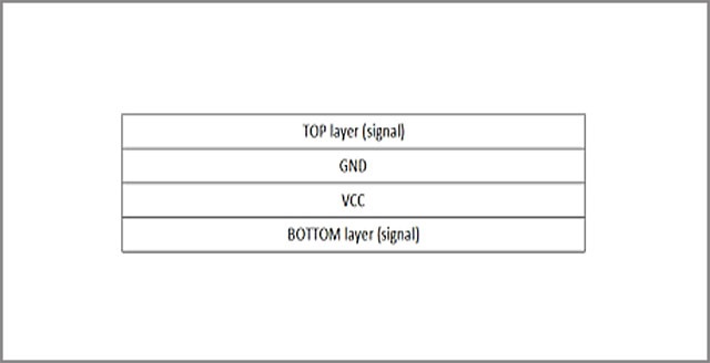
- Stacking: This is one of the basic elements of multi-layer PCB design. Layering is the number and sequence of PCB design layers. Most manufacturers can support up to 16 sheets of paper. The most common four - and six-layer PCB stacks are shown in the bottom of Figure 1 and Figure 2. The four-tier stack consists of the top and bottom layers (signal layer) with GND and VCC (power layer) in between. A six-layer stack is the same as a four-layer stack, except that between the power layers are two other signal layers (for example, high speed).
Figure 1 Four-layer PCB stack

Figure 2 Six-layer PCB stack

For high-speed signals, as shown in Figure 2, six-layer PCB laminations are a better solution than four-layer PCB laminations because high-speed signals are more isolated and EMI is reduced for this design.
Through-holes: Although through-holes are required, it is best to use only through-holes as this will make the design more cost effective. Multilayer PCB designs can also use blind holes if they cannot be buried. The buried hole connects the inner layer, and the blind hole is only exposed to one of the two outer layers of the PCB.
An example is a PCB design involving a BGA (ball-grid array) IC, where a multilayer PCB design is almost always required due to BGA escaping the wiring, which is to route the wiring from the BGA chip to the rest of the PCB.
2. PCBA maintenance in SMT patch processing
In the production and use process of SMT patch processing, problems occur in the whole PCBA manufacturing process and use process, including processing errors, improper use, aging of components and other factors, which may lead to abnormal work or even poor use of the real product. Because many products just don't need to be replaced completely. This requires certain repair and maintenance of the circuit board inside. Then it involves the maintenance of the circuit board! Today, kingford is here to briefly share some experience and skills in circuit board maintenance technology. If you want to systematically learn circuit board maintenance technology, you can click on the official website of Jingbang Electronics. We will regularly share some practical tips in SMT processing plant, including but not limited to maintenance:
Generally, the maintenance technology unit in our patch processing plant will carry out the following operations.
1. Check components
In SMT patch factory, when the products need to be repaired, it is necessary to first confirm whether there are any problems of error, leakage and reverse of the components of each solder joint. It is also necessary to confirm the authenticity of no materials. Since Jingbang Electronics imported chips from Sweden in 2011, the source of goods in European and American countries may not be all stronger than Huaqiangbei. If you eliminate the problem of error, leakage, reverse and authenticity, you can get a faulty circuit board first check whether the circuit board is intact, whether each component is obviously burned out or not.
2. Welding state analysis
Basically 80% of the defects of circuit boards are defects of solder joints. If the solder joints are full and abnormal, we should first refer to the management standards of ISO9001 quality system and various SMT welding quality standards to check whether there are defects visible to the naked eye such as virtual welding, false welding, short circuit, and whether the copper skin is obviously cocking. If yes, we need to repair the defective points of this product. If not, we can proceed to the next step.
3. Detection of component direction
In the process of this link, we have basically eliminated some bad things that can be seen by the naked eye. Now we still need to carefully check whether the diodes, electrolytic capacitors, which are the most used components on the circuit board, and other components that have provisions on the direction, or positive and negative electrode requirements are inserted in the wrong direction.
4. Tool testing of components
If all the naked eye judgment is no problem, at this time we need to borrow some auxiliary tools, SMT patch factory is the most commonly used to use a multimeter to simply measure our resistance, capacitance, audion and other components, the main test with a multimeter is to check whether the resistance value of these components is not in line with the normal value. Bigger or smaller, whether the capacitor is open, whether the inductor is open, and so on.
5. Power-on test
After all the above process is completed, basically can eliminate the conventional problems of components, power will not be because of short circuit or bridge and other circuit board ablative damage. You can switch on the power supply and check whether the corresponding function of the circuit board is normal
Basically, after the completion of all processes, defects of customers' products can be judged and repaired based on customers' BOM, Gerber and schematic diagrams. In the patch processing plant, our maintenance department technicians are all professionals carefully selected from the workshop.


Just upload Gerber files, BOM files and design files, and the KINGFORD team will provide a complete quotation within 24h.