
Professional PCB manufacturing and assembly
Building 6, Zone 3, Yuekang Road,Bao'an District, Shenzhen, China
+86-13410863085Mon.-Sat.08:00-20:00

A few pictures of BGA solder, sliced from my own products, are used as teaching materials, and there are typical double balls (HIP, Head-In-Pillow) and pictures of tin balls being pulled. Usually when you get a BGA slice photo, the first thing to judge is which side belongs to the packaging surface of BGA and which side belongs to the circuit board assembly surface. The following patch processing manufacturers will explain the knowledge about how to judge the welding quality of BGA slices and how to design PCB from the Angle of patch welding.
1. How to design PCB from the Angle of patch welding
With the rapid development of electronic technology, electronic components of miniaturization, miniaturization, BGA, spacing of 0.3mm~0.5mm high density chip is becoming more and more common, the requirements of electronic welding technology is becoming higher and higher. Although there are now more sophisticated SMT machines can replace manual welding, but there are too many factors affecting the quality of welding. From the point of view of patch welding, this paper introduces some points that need to be paid attention to when designing PCB. According to experience, if these requirements are not followed, it is likely to cause poor welding quality, virtual welding and even damage the pad or circuit board when repairing PCB.
1. Factors affecting PCB welding quality From PCB design to the completion of welding of all components into a high quality circuit board, PCB design engineers and even the level of welding technology, welding workers and many other links have strict control. There are mainly the following factors: PCB diagram, the quality of the circuit board, the quality of the device, the oxidation degree of the device pin, the quality of the solder paste, the printing quality of the solder paste, the accuracy of the program of the placement machine, the mounting quality of the reflow furnace temperature curve setting and so on. SMT patch welding plant itself cannot surmount the link is PCB drawing link. Because people who do circuit design often do not weld circuit boards so that they can not get direct welding experience, do not know the various factors affecting welding; However, the workers in SMT welding factory do not know the design of PCB drawing board. They just finish the production task without thinking or ability to analyze the causes of bad welding. Due to the two aspects of the talent in their respective roles, it is difficult to organically combine.
In the following, I propose some suggestions to the design and wiring engineers who draw PCB drawings in the process of PCB drawing, hoping to avoid all kinds of bad drawings that affect welding quality in the process of drawing. Will be introduced mainly in the form of graphics.
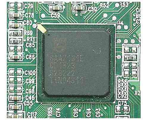
2. How to judge the welding quality of BGA slices
This article is basically for those of you who still don't know how to judge whether sliced BGA is good or bad. Because I happen to have a few BGA solder pictures of my own products sliced, which can be used as a textbook, and also have the typical double ball (HIP, Head-In-Pillow) and the picture of the tin ball being pulled. Usually when you get a BGA slice photo, the first thing to judge is which side belongs to the packaging surface of BGA and which side belongs to the circuit board assembly surface. For this problem, my method is to judge from the thickness of copper foil. The thicker side of copper foil is usually the circuit board assembly surface, because the carrier board of BGA packaging is usually thinner than the circuit board of electronic assembly, so the thinner thickness of copper foil will be chosen.
Secondly, if the double ball phenomenon can be clearly seen (the following picture shows the typical shortcomings of HIP pseudo-cold welding), the larger side of the ball is usually the original tin ball on the carrier plate, because the volume of the BGA tin ball has been Reflow. On the other hand, the solder paste printed on PCB is only half of its original volume after a Reflow flux volatilization, so the spheres on BGA are usually larger. As for the size of welding Pad (pad) is not necessarily, it depends on whether your PCB layout Design adhere to the design of Cooper Define Pad Design (copper foil independent pad design). Then judging the quality of BGA welding, the following figure can clearly see the typical [double ball (HIP)] welding problem, those who do not understand can click the "HIP(Head-in-Pillow effect)" link for further discussion, 99% HIP should occur on the outer row of tin balls around the BGA. The cause is almost always the deformation and warping of BGA carrier plate or PCB after Reflow, and the deformation becomes smaller after the board is returned to temperature, but the molten tin has cooled, thus forming the appearance of two balls together. HIP is a serious BGA solder defect, it is easy to pass through the factory testing procedures to the customer's hands, but after a period of use, the product will be sent back for repair due to problems.
The second kind of bad BGA solder is the tin ball between HIP and normal solder. Do you know how to judge which side is PCB end? From below BGA solder ball and solder paste on the PCB has been completely fused together, because can't see the double ball, but the whole tin ball has been up and down spin and almost broken signs, observed on the surface of the PCB soldering tin can also find the ball contact with PCB soldering pad area is smaller, but also appears no ð « » long point of view, this is because the tin ball is the pull up This kind of solder fracture should only be a matter of time, the client should be used when the vibration or switching process of thermal expansion and cold contraction, will accelerate its fracture. The welding of BGA tin ball in the following picture is acceptable. The ball can also be flattened to form horizontal oval solder, but it is still visible that the tin ball near the PCB end is somewhat pulled apart. In fact, a good solder ball shape should be like the picture below, the tin ball resembles a "lantern shape", the tin ball covers the entire PCB welding pad. Sometimes, however, the pad is designed to be covered with green oil, and the shape will look more like the picture above.
How do PCB design digital analog connect
Feb 08,2023


Just upload Gerber files, BOM files and design files, and the KINGFORD team will provide a complete quotation within 24h.