
Professional PCB manufacturing and assembly
Building 6, Zone 3, Yuekang Road,Bao'an District, Shenzhen, China
+86-13410863085Mon.-Sat.08:00-20:00

Layout is an important part of design. The result of layout will directly affect the effect of wiring, so it can be considered that a reasonable layout is the first step of successful PCB design.
Prelayout, in particular, is the process of thinking about the entire circuit board, signal flow, heat dissipation, structure and other structures. If the pre-layout is a failure, the subsequent efforts will be wasted.
1. Think big
The success of a product, one is to pay attention to the internal quality, two is to take into account the overall beauty, both are more perfect in order to consider the product is a success.
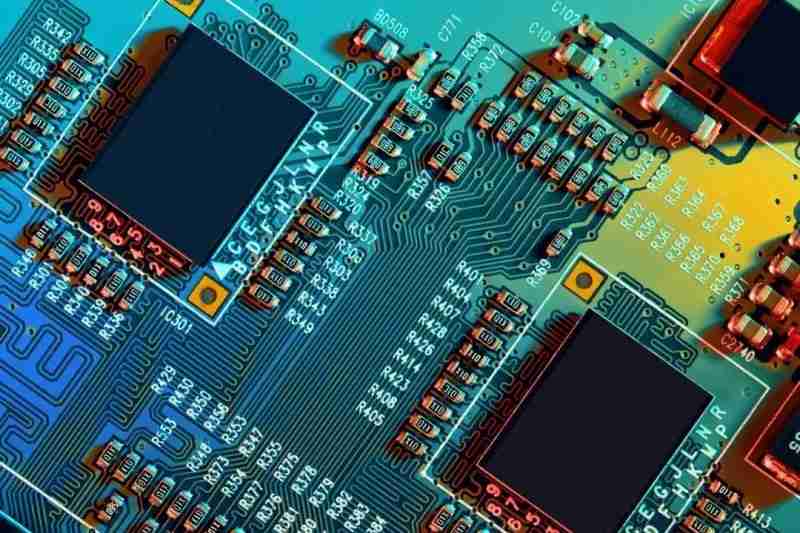
On a PCB board, the layout of components is required to be balanced, dense and orderly, not top-heavy or heavy.
Will the PCB be deformed?
Are craft edges reserved?
Are MARK points reserved?
Do you need a board?
How many layers can guarantee impedance control, signal shielding, signal integrity, economy, realizability?
2. Eliminate silly mistakes
Are the dimensions of the printed board consistent with those of the machined drawings? Can it meet the requirements of PCB manufacturing process? Is there a location marker?
Does the component conflict in two - and three-dimensional space?
Is the component layout dense and orderly? Is it all done?
Can frequently replaced components be easily replaced? Is the plug-in board easy to plug into the device?
Is there a proper distance between the thermal element and the heating element?
Is it convenient to adjust the adjustable element?
Are radiators installed where heat is needed? Is the air flow smooth?
Is the signal flow smooth with minimal interconnection?
Are plugs, receptacles, etc. inconsistent with mechanical design?
Is line interference considered?
3. Bypass or decoupling capacitor
Both simulator and digital devices require these types of capacitors when wiring, and both need to connect a bypass capacitor, typically 0.1μF, close to their power supply pins. The pin should be as short as possible to reduce the inductance of the wire, and should be as close to the device as possible
The addition of bypass or decoupling capacitors to the circuit board, and the placement of these capacitors on the board, is common sense for both digital and analog design, but the function is different. In analog wiring design, bypass capacitors are usually used for high frequency signals on the bypass power supply. Without bypass capacitors, these high frequency signals may enter the sensitive analog chip through the power supply pins. In general, the frequency of these high-frequency signals exceeds the capability of the simulator to suppress the high-frequency signals. If bypass capacitors are not used in an analog circuit, noise may be introduced along the signal path, or even vibration may be caused in worse cases. For digital devices such as controllers and processors, decoupling capacitors are also needed, but for different reasons. One function of these capacitors is to be used as a "miniature" charge library. This is because in digital circuits, performing the switching of gate states (i.e., switching) usually requires a large current, and it is advantageous to have this extra "backup" charge when switching creates a switching transient current on the chip and flows through the circuit board. If the switching action is performed without sufficient charge, it will cause a large change in the supply voltage. The change of electric voltage is too large, the digital signal level will enter the uncertain state, and it is likely to cause the state machine error operation in the digital device. Switching current flowing through circuit board wiring will cause voltage changes. Since there is parasitic electric sensation in circuit board wiring, the following formula can be used to calculate voltage changes: V=Ldl/dt where V= change in voltage L= inductive reactance of circuit board wiring dI= change in current flowing through the wiring dt= time of current change Therefore, it is very good practice to apply bypass (or decoupling) capacitors at the supply source or at the power pin of the active device for a variety of reasons.
4, input power supply, if the current is relatively large, it is recommended to reduce the length and area of the line, do not run the field
The switching noise on the input is coupled to the plane of the power output. The switching noise of the MOS tube of the output power supply affects the input power supply of the preceding stage.
If there are a lot of high current DCDC on the circuit board, there are different frequencies, high current and high voltage jump interference.
So we need to reduce the area of the input power supply to meet the current. So when the power supply layout, to consider avoiding the input power full board run.
5. Power cables and ground cables

The positions of power cables and ground cables are well coordinated to reduce the possibility of electromagnetic interference (EMl). If the power cable and ground cable are not properly matched, the system loop will be designed and may generate noise. The PCB design example of improper combination of power cable and ground cable is shown in the figure. On this circuit board, different routes are used to distribute the power cord and ground wire. Because of this improper match, the electronic components and circuits of the circuit board are subject to electromagnetic interference (EMI).
6, digital separation
In each PCB design, the noisy and "quiet" (non-noisy) parts of the circuit are separated. Generally speaking, digital circuits can tolerate noise interference and are not sensitive to noise (because digital circuits have a large voltage noise tolerance); In contrast, the voltage noise tolerance of an analog circuit is much smaller. Of the two, the analog circuit is the most sensitive to switching noise. In the wiring of a mixed-signal system, the two circuits are separated.
The basic knowledge of circuit board wiring applies to both analog and digital circuits. A basic rule of experience is to use an uninterrupted ground plane. This basic rule reduces the dI/dt effect in digital circuits, because the dI/dt effect causes the potential of the ground and introduces noise into analog circuits. The wiring techniques for digital and analog circuits are basically the same, except for one thing. For analog circuits, also need to pay attention to another point, is to put the digital signal line and ground plane circuit as far away from the analog circuit. This can be achieved by either connecting the analog ground plane individually to the systematic connection, or by placing the analog circuit at the farthest end of the board, the end of the line. This is done to keep the signal path to a minimum of external interference. This is not necessary for digital circuits, which can tolerate large amounts of noise in the ground plane without problems.
7, heat dissipation consideration
In the PCB layout process, need to consider the heat dissipation duct, heat dissipation dead Angle;
Do not place heat-sensitive devices behind heat sources and wind. Give priority to the layout of DDR such as heat dissipation difficulties. Avoid repeated adjustment due to failure of thermal simulation.


Just upload Gerber files, BOM files and design files, and the KINGFORD team will provide a complete quotation within 24h.