
Professional PCB manufacturing and assembly
Building 6, Zone 3, Yuekang Road,Bao'an District, Shenzhen, China
+86-13410863085Mon.-Sat.08:00-20:00

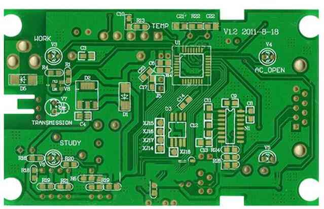
For electronic devices, a certain amount of heat is generated during operation, which rapidly raises the internal temperature of the device. If the heat is not released in time, the device will continue to heat, and the device will fail due to overheating, and the reliability of the electronic device will be reduced. Therefore, good heat dissipation treatment is very important in PCB design. Next, we introduce how to improve the heat dissipation performance of PCB design. The following patch processing manufacturer Xiaobian to explain how to improve the heat dissipation performance of PCB circuit board and SMT patch processing how to check the quality of spot welding knowledge.
How to check spot welding quality in SMT patch processing
Nowadays, in order to meet market demand, most electronic devices are moving towards precision machining and practical application. Even so, the electronic components of PCB circuit boards are getting smaller and smaller, and the assembly accuracy requirements are also getting higher and higher. Electronic processing plants often need to use SMT SMT processing technology to meet the needs of projects. As a direct result of electric welding, the quality and reputation of spot welding determines the quality of electronic equipment. How to ensure the quality of spot welding in SMT patch processing is a never-ending problem for electronic processing factories and SMT engineers. We also put forward many constructive suggestions and methods. So, how to check the SMT patch processing spot welding quality?
First, SMT spot welding inspection:
1. The surface must be fine, smooth and bright, without defects; 2. The component aspect ratio shall be moderate, and there shall be an appropriate amount of welding materials and welding materials to completely cover the welding position of the welding plate and lead; 3. Excellent wettability. The edges of the welding points should be relatively thin.
Ii. Contents to be checked for SMT production and machining appearance:
1. Whether to ignore this element; 2. Are components mounted correctly? 3. Check whether a short-circuit fault occurs. 4. The component is not securely connected because it is virtual. Generally speaking, SMT patch processing should be carried out appearance inspection to ensure the quality of electronic equipment under the premise of fine spot welding of mechanical equipment and effective characteristics of mechanical and electrical equipment. SMT SMT manufacturing industry as the basis of electronic equipment manufacturing, so what factors will damage the quality of SMT SMT manufacturing? A subtle key point and manufacturing stage will lead to large and small product quality issues, inspection failures, delivery delays, etc.
3. Factors that harm the quality of SMT patches and lead to the lack of parts in the patch program are as follows:
1. feeder of electronic equipment (feeder) cannot be fed timely; 2. The vacuum sucker of the component is blocked by the air supply and damaged by the vacuum sucker, and the ratio between the vacuum sucker and the width is incorrect; 3. Common failures and blockages of the real gas path of machines and equipment; 4. The circuit board is not picked up properly, resulting in deformation; 5. No welding paste or too little welding paste on the circuit board welding plate; 6. Electronic equipment product quality problems, the same thickness is not consistent; 7. There are defects in the application process of the patch machine, or the major parameters of the thickness of the electronic equipment are not correctly selected when the program is written; 8. Human error accidentally knocked it down.

How to improve the heat dissipation performance of PCB circuit board
1. The larger the contact area is, the lower the junction temperature is; 2. The larger the copper covering area, the lower the junction temperature.
The addition of hot pass holes in PCB design can effectively reduce the junction temperature of the device and improve the temperature uniformity in the direction of the thickness of the board, which provides the possibility of using other heat dissipation methods on the PCB back. Through simulation, it is found that compared with the device without heat dissipation hole, the thermal power consumption of this device is 2.5W, the spacing is 1mm, the center design is 6x6, the junction temperature can be reduced by about 4.8°C, and the temperature difference between the top and bottom of the PCB is reduced from 21°C to 5°C. By changing the hot-through-hole array to 4X4, the junction temperature of the device is 2.2°C higher than that of 6x6, which is noteworthy.
Three, PCB design IC back exposed copper, reduce the thermal resistance between copper and air.
4. PCB design and layout optimization Requirements for PCB design and layout of high-power and thermal equipment.
1. Place the heat-sensitive equipment in the cold air area. 2. The temperature detection device should be placed in the hottest position. 3. In the same piece of PCB device should be as far as possible according to the size of heat and heat distribution degree, small heat or poor heat resistant devices (such as small signal transistors, small integrated circuits, electrolytic capacitors, etc.) cooling airflow is best at the entrance, large heat or good heat resistant devices (such as power transistors, large-scale integrated circuits, etc.) of the most downstream cooling airflow. 4. In the horizontal direction, the high-power equipment should be arranged as close as possible to the edge of the PCB board to shorten the heat transfer path; In the vertical direction, high-power components should be arranged as close to the top of the printed circuit board as possible to reduce the impact of these components on the temperature of other components when operating. 5. The heat dissipation of the printed circuit board in the equipment mainly depends on the air flow, so it is necessary to study the air flow path in the design and reasonable configuration of the equipment or printed circuit board. Air flow tends to flow in areas with low resistance. Therefore, when configuring devices on a printed circuit board, avoid leaving large Spaces in the area. The same problem should be noted for the configuration of multiple printed circuit boards throughout the machine. 6. It is better to place the temperature-sensitive device in the area with the lowest temperature (such as the bottom of the device) rather than directly above the heating device. It is better to place multiple devices in a horizontal staggered layout. 7. The equipment with the highest power consumption and heat is located near the optimal heat dissipation location. Do not place high-temperature devices in the corners and edges of printed circuit boards unless a radiator is nearby. In the design of power resistance should be as large as possible to choose the device, and adjust the PCB design layout, so that it has enough space for heat dissipation.
The highest signal design rate: 10Gbps CML differential signal; Maximum number of PCB design layers: 40; Minimum line width: 2.4mil; Minimum line spacing: 2.4mil; Minimum BGA PIN spacing: 0.4mm; Minimum mechanical hole diameter: 6mil; Minimum laser drilling diameter: 4mil; Maximum number of pins:; 63000+ Max number of components: 3600; Maximum number of BGA: 48+. 1. The customer provides schematic diagram to consult PCB design; 2. Evaluate quotation according to schematic diagram and customer design requirements; 3. The customer confirms the quotation, signs the contract and pays the project deposit; 4. Received advance payment and arranged engineer design; 5. After the design is completed, provide the screenshot of the document to the customer for confirmation; 6. The customer confirmed OK, settled the balance, and provided PCB design materials
Rf circuit PCB design skills
Feb 05,2023


Just upload Gerber files, BOM files and design files, and the KINGFORD team will provide a complete quotation within 24h.