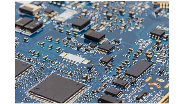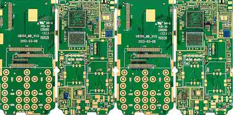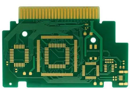
The difficulty of PCB design is that there are more and more devices with different digital logic, such as GTL, LVTTL, LVCMOS and LVDS logic. The logic threshold and voltage swing of each logic circuit are different. However, these circuits with different logic threshold and voltage swing must be jointly designed on a PCB multilayer circuit board.

Fundamentals of mixed signal circuit wiring
When digital and analog circuits share the same components on a unified block board, the circuit layout and wiring must be methodical.
In mixed-signal printed circuit board design, there are special requirements for power wiring and the isolation of analog and digital noise from each other to avoid noise coupling, which increases the complexity of layout and wiring. The special requirements for power transmission lines and the need to isolate noise coupling between analog and digital circuits add further complexity to the layout and wiring of mixed-signal printed boards.
If the power supply of the analog amplifier in A/D converter and the digital power supply of A/D converter are connected together, it is likely to cause the interaction of the analog and digital circuits. Perhaps, because of the position of the input/output connectors, the layout plan must mix the wiring of the digital and analog circuits.
Before the layout and wiring, the engineer should understand the basic weaknesses of the layout and wiring scheme. Even in the presence of false determinations, most engineers tend to use layout and wiring information to identify latent electrical effects.
Layout and wiring of modern mixed signal printed circuit boards
The following will elaborate the mixed signal printed circuit board layout and wiring technology through the design of OC48 interface card. OC48 stands for optical carrier scale 48, which is basically oriented to 2.5Gb serial optical communication. It is a kind of optical communication scale with high capacity in modern communication equipment. The OC48 interface card contains several typical mixed-signal printed circuit board layout and wiring problems. The layout and wiring process will indicate the sequence and steps to solve the mixed-signal printed circuit board layout solution.

The OC48 card contains an optical transceiver that realizes the bidirectional conversion of optical signals and analog electrical signals. Analog signals input or output digital signal processors, and the DSP converts these analog signals into digital logic levels that can be connected to the microprocessor, the programmable gate array, and the DSP and microprocessor's system interface circuits on the OC48 card. Separate PLLS, power filters, and local reference voltage sources are also integrated.
Among them, the microprocessor is a multi-power device, the main power is 2V, and the 3.3V I/O signal power is shared by other digital devices on the board. An independent digital clock source provides clocks for OC48I/O, microprocessors, and system I/O.
After checking the layout and wiring requirements of different functional circuit board, 12-layer board is preliminarily recommended, as shown in Figure 3. The configuration of the microstrip and strip line layers can safely reduce the coupling of adjacent line layers and improve impedance control. The grounding layer between the first layer and the second layer isolates the wiring of the sensitive analog reference source, CPU core and PLL filter power supply from the microprocessor and DSP devices in the first layer. The power supply and connection layer are always paired, as is done for the shared 3.3V power layer on the OC48 card. This will reduce the impedance between the power source and the ground, thus reducing the noise on the power signal.
Avoid running digital clock lines and high frequency analog signal lines near the power layer, or the noise from the power signal will be coupled to the sensitive analog signal.
Careful consideration should be given to the use of power and analog splits, especially in the input and output of mixed-signal devices, as required for digital signal wiring. Running through a gear near the signal layer can result in discontinuous impedance and poor transmission line loops. All of this causes signal quality, timing, and EMI problems.


