
Professional PCB manufacturing and assembly
Building 6, Zone 3, Yuekang Road,Bao'an District, Shenzhen, China
+86-13410863085Mon.-Sat.08:00-20:00

SMT patch processing, namely surface mounting technology, specifically refers to the technology of placing wafer structure components or miniaturized components suitable for surface assembly on the surface of PCB according to requirements, and then welding them together by reflow welding and other welding technologies to complete the assembly of electronic components. On SMT circuit board, solder joints and components are on the same plane of the circuit board, so in SMT processing PCB, through holes are only used to connect the wires on both sides of the circuit board, the number of holes is much less, and the diameter of holes is much smaller. This design can greatly improve the installation density of PCB components.
1. Miniaturization
The size and volume of SMT sheet components are much smaller than traditional plug-in components, which can be reduced by 60% ~ 70% or even 90%. The weight is reduced by 60% ~ 90%. This can meet the development needs of miniaturization of electronic products.
2. High signal transmission speed
SMT PCB processing compact structure, high installation density, can achieve short connection, small delay effect, so as to achieve high-speed signal transmission. At the same time, it can make electronic products more resistant to vibration and shock.
3. High frequency characteristics
SMT machining of components usually has no leads or short leads, which reduces circuit distribution parameters and thus RF interference.
4. It is conducive to automated production
SMT chip components have many characteristics, such as size standardization, serialization and consistency of welding conditions, which can make SMT chip machining highly automatic.
5. Low material cost
The packaging cost of components is lower than that of components of the same type and function.
6. High production efficiency
SMT mounting technology simplifies the production process of electronic products and reduces the production cost. Shorten the whole production process, improve the production efficiency.
Circuit board names are: ceramic circuit board, alumina ceramic circuit board, aluminum nitride ceramic circuit board, circuit board, PCB board, aluminum substrate, high frequency board, thick copper plate, impedance board, PCB, ultra-thin circuit board, ultra-thin circuit board, printing (copper etching technology) circuit board, etc. The circuit board makes the circuit miniaturized and intuitive, which plays an important role in the mass production of fixed circuit and the optimization of electrical appliance layout. Circuit boards may be called printed circuit boards or printed circuit boards, The English name is (Printed Circuit Board) PCB, (Flexible Printed Circuit) FPC circuit board (FPC circuit board also known as flexible circuit board) Flexible circuit board is made of polyimide or polyester film as a substrate with high reliability of flexible printed circuit board. It has the characteristics of high wiring density, light weight, thin thickness and good bending. and Soft and hard combination plate (reaches, soft and hard combination plate) - the birth and development of FPC and PCB, gave birth to the soft and hard combination plate this new product. Therefore, the combination of soft and hard board, is the flexible circuit board and hard circuit board, after pressing and other processes, according to the relevant process requirements combined together, the formation of a circuit board with FPC characteristics and PCB characteristics.

The core of the high-density interconnection board (HDI) is in the through hole
Multi-layer PCB line processing, and single layer and double layer no difference, the biggest difference in the hole process.
Lines are etched out, holes are drilled and then copper plated out, these do hardware development we all understand, do not repeat.
Multilayer circuit board, usually through the hole plate, first board, second board, second stack plate these several. Higher level such as the third level board, arbitrary layer interconnection board usually used very little, the price thief expensive, not to discuss.
Under normal circumstances, 8-bit single-chip microcomputer products with 2 layers of through hole plate; 32-bit single-chip level intelligent hardware, using 4-6 layers of through hole plate; Linux and Android level smart hardware, using 6-layer through hole to 8 first-stage HDI boards; Smart phone such compact products, generally use 8 layers of the first level to 10 layers of the second level circuit board.
The most common through-hole.
There is only one perforation, from the first layer to the last layer. No matter the external line or the internal line, the hole is pierced, called through hole plate.
Through the hole plate and the number of layers does not matter, usually we use 2 layers are through the hole plate, and many switches and military circuit boards, do 20 layers, or through the hole.
The circuit board is drilled through with a drill and copper plated in the holes to create a path.
Note that the inner diameter of the through hole is usually 0.2mm, 0.25mm and 0.3mm, but generally 0.2mm is much more expensive than 0.3mm. Because the drill bit is too thin and easy to break, the drill is also slower. The extra time and drill costs are reflected in the rising price of circuit boards.
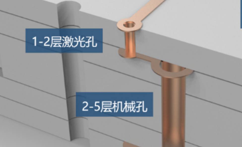
Laser hole of high density board (HDI board)
This figure shows the laminated structure of 6 layers of 1 order HDI board. The two layers on the surface are laser holes with 0.1mm bore. The inner layer is a mechanical hole, equivalent to a 4-layer through hole plate, and the outside is covered with 2 layers.
Lasers can only Pierce fiberglass plates, not metal copper. So the outer surface punching will not affect the other lines inside.
After the laser hole is punched, the copper is plated, and the laser hole is formed.
Two layers of laser holes on a 2-stage HDI board.
This is a 6 - layer 2 - order staggered HDI board. Usually we use 6 layers of 2 less, most of the 8 layers of 2. There are more layers here, same thing as six layers.
The so-called second order, there are two layers of laser holes.
The so-called wrong hole, is the two layers of laser holes are staggered.
Why stagger it? Because the copper plating is not satisfied, the hole inside is empty, so it can not be directly punched on the above, to stagger a certain distance, and then hit a layer of empty.
Six levels of second order is equal to four levels of first order plus two levels.
Eight levels of second order is equal to six levels of first order plus two levels.
Laminated plate technology is complex and the price is higher.
The two layers of laser holes in the staggered plate overlap. The line will be tighter.
The inner laser hole needs to be electroplated and filled, and then the outer laser hole is made. The price is more expensive than the error hole.
Super expensive multi - layer laser hole - stacking of arbitrary - layer inter connectors.
Each layer is a laser hole, and each layer can be connected together. Line the line however you want, punch the hole however you want.
Layout engineers think about it! No longer afraid not to draw!
Purchasing just think about crying, more than 10 times more expensive than the ordinary through hole plate!
What are the commonly used PCB design software?
Jan 28,2023


Just upload Gerber files, BOM files and design files, and the KINGFORD team will provide a complete quotation within 24h.