
Professional PCB manufacturing and assembly
Building 6, Zone 3, Yuekang Road,Bao'an District, Shenzhen, China
+86-13410863085Mon.-Sat.08:00-20:00

1、 Design of PCB
1. PCB pad design
(1) When designing the pad of plug-in components, the pad size shall be designed appropriately. The pad is too large, the solder spreading area is large, and the solder joints formed are not full, while the surface tension of the copper foil of the smaller pad is too small, and the solder joints formed are non wetting solder joints. The fit gap between the hole diameter and PCB component lead is too large, which is easy to solder. When the hole diameter is 0.05 - 0.2mm wider than the lead, and the pad diameter is 2 - 2.5 times of the hole diameter, it is an ideal condition for welding.
(2) When designing the bonding pad of SMD components, the following points should be considered: In order to eliminate the "shadow effect" as far as possible, the SMD terminal or pin should face the direction of the tin flow to facilitate the contact with the tin flow and reduce false soldering and solder skips. The smaller components shall not be arranged behind the larger components, so as to prevent the larger components from hindering the contact between the tin flow and the pad of the smaller components and causing solder leakage.
2. Flatness control of pcb proofing
Wave soldering has high requirements on the flatness of printed boards. Generally, the warpage should be less than 0.5mm. If it is greater than 0.5mm, leveling should be done. In particular, if the thickness of some printed boards is only about 1.5mm, the requirements for warpage are higher. Otherwise, the welding quality cannot be guaranteed. The following matters should be noted:
(1) Properly store printed boards and components, and shorten the storage period as much as possible. During welding, copper foil and component leads free of dust, grease and oxide are conducive to forming qualified solder joints. Therefore, printed boards and components should be stored in a dry and clean environment, and the storage period should be shortened as much as possible.
(2) For printed boards that have been placed for a long time, their surfaces should generally be cleaned to improve solderability and reduce false soldering and bridging. For component pins with a certain degree of oxidation on the surface, the surface oxide layer should be removed first.
2、 Quality control of process materials
In wave soldering, the main process materials used are: flux and solder.
1. The application of flux can remove the oxide on the welding surface, prevent the re oxidation of solder and welding surface during welding, reduce the surface tension of solder, and help heat transfer to the welding area. Flux plays an important role in the control of welding quality. At present, most of the wave soldering fluxes are non cleaning fluxes, and the following requirements apply when selecting fluxes:
(1) The melting point is lower than that of solder;
(2) The infiltration and diffusion speed is faster than that of melted solder;
(3) Viscosity and specific gravity are smaller than solder;
(4) Stable storage at room temperature.
2. Quality Control of Solder
The tin lead solder is continuously oxidized at high temperature (250 ℃), which makes the tin content of tin lead solder in the tin pot continuously decrease, deviates from the eutectic point, resulting in poor liquidity, continuous soldering, faulty soldering, insufficient solder joint strength and other quality problems. The following methods can be used to solve this problem:
(1) Add oxidation-reduction agent to reduce oxidized SnO to Sn and reduce the production of tin slag.
(2) Add a certain amount of tin before each welding.
(3) Solder containing oxidation resistant phosphorus shall be used.
(4) Nitrogen protection is used to isolate the solder from the air and replace the ordinary gas, thus avoiding the generation of scum.
The current method is to use phosphorus containing solder in the atmosphere of nitrogen protection, which can control the scum rate at a low level, with fewer welding defects and better process control.
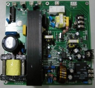
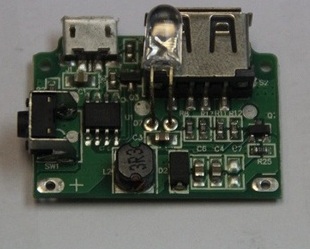
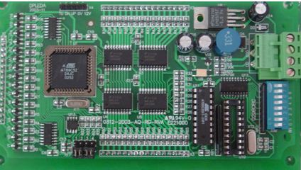
Pcb board proofing
3、 Welding PCB process parameter control
The influence of welding process parameters on the quality of welding surface is relatively complex, mainly including the following points:
1. Control of preheating temperature
Preheating effect: ① Make the solvent in the flux volatilize sufficiently to avoid affecting the wetting of the PCB and the formation of solder joints when the PCB passes through the soldering tin; ② Make the printed board reach a certain temperature before welding to avoid warping deformation caused by thermal shock. According to our experience, the preheating temperature is generally controlled at 180 200 ℃ and the preheating time is 1 - 3 minutes.
2. Inclination of welding track
The influence of rail inclination on welding effect is obvious, especially when welding high-density SMT devices. When the inclination angle is too small, bridging is more likely to occur, especially in the "shielding area" of SMT devices during welding; However, if the inclination angle is too large, although it is conducive to the elimination of bridging, the solder consumption of solder joints is too small, which is prone to false soldering. The rail inclination shall be controlled between 5 ° and 7 °.
3. Crest height
The height of the wave crest will change due to the passage of the welding working time. Proper correction should be made during the welding process to ensure the ideal height of the wave crest for welding. The tin pressing depth should be 1/2 - 1/3 of the PCB thickness.
4. Welding temperature
Welding temperature is an important process parameter that affects welding quality. When the welding temperature is too low, the expansion rate and wettability of the solder become poor, so that the solder pad or component solder end can not be fully wetted, resulting in defects such as false soldering, tip pulling, bridging, etc; If the welding temperature is too high, the oxidation of bonding pads, component pins and solder will be accelerated, which is easy to cause false soldering. Generally speaking, the welding temperature should be controlled at 250+5 ℃.
So far as the quality control method of pcb board proofing is concerned today. Welding is an important process step in pcb proofing process. in order to ensure the welding quality of pcb, we should master the quality control methods and welding skills.


Just upload Gerber files, BOM files and design files, and the KINGFORD team will provide a complete quotation within 24h.