
Professional PCB manufacturing and assembly
Building 6, Zone 3, Yuekang Road,Bao'an District, Shenzhen, China
+86-13410863085Mon.-Sat.08:00-20:00

The goal of PCB design is smaller, faster and lower cost. As the interconnection point is the weakest link in the circuit chain, in RF design, the electromagnetic property at the interconnection point is the main problem faced by engineering design. It is necessary to investigate each interconnection point and solve the existing problems.
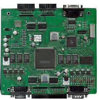
The interconnection of circuit board system includes chip to circuit board, interconnection within PCB board and signal input/output between PCB and external devices. This paper mainly introduces the summary of practical skills of high frequency PCB design by interconnecting PCB boards. I believe that understanding this paper will bring convenience to PCB design in the future.
In PCB design, the interconnection between chips and PCBs is important for design. However, the main problem of the interconnection between chips and PCBs is that too high interconnection density will lead to the basic structure of PCB materials becoming a factor limiting the growth of interconnection density. This paper shares the practical skills of high-frequency PCB design.
As far as high-frequency applications are concerned, the techniques for designing high-frequency PCBs by interconnecting PCBs are as follows:
1. 45 ° angle shall be adopted for transmission line corner to reduce return loss;
2. High performance insulated circuit boards with strictly controlled insulation constant values shall be used. This method is conducive to effective management of electromagnetic fields between insulating materials and adjacent PCB wiring.
3. PCB design specifications for high-precision etching should be improved. Consider that the total error of the specified line width is+/-0.0007 inches, manage the undercut and cross section of the wiring shape, and specify the electroplating conditions of the wiring sidewall. The overall management of wiring (wire) geometry and coating surface is very important to solve the skin effect problem related to microwave frequency and realize these specifications.
4. There is tap inductance in the protruding leads, so avoid using components with leads. In high-frequency environment, it is better to use surface mounted PCB components.
5. For signal vias, it is necessary to avoid using the through hole machining (pth) process on sensitive plates. This process will lead to lead inductance at the via. If a via on a 20 layer board is used to connect layers 1 to 3, the lead inductance can affect layers 4 to 19.
6. Abundant ground plane shall be provided. The molded holes shall be used to connect these grounding layers to prevent the influence of 3D electromagnetic field on the circuit board.
7. The non electrolytic nickel plating or gold immersion plating process shall be selected, and the HASL method shall not be used for electroplating. The electroplating surface can provide better skin effect for high-frequency current. In addition, this highly weldable coating requires fewer leads, which helps reduce environmental pollution.
8. PCB solder mask prevents solder paste from flowing. However, due to the uncertainty of thickness and the uncertainty of insulation performance, covering the entire plate surface with solder resistance materials will lead to a large change in electromagnetic energy in microstrip design. Solder dam is generally used as PCB solder mask.
Are PCB design layers mostly even
Jan 04,2023


Just upload Gerber files, BOM files and design files, and the KINGFORD team will provide a complete quotation within 24h.