
Professional PCB manufacturing and assembly
Building 6, Zone 3, Yuekang Road,Bao'an District, Shenzhen, China
+86-13410863085Mon.-Sat.08:00-20:00

High speed backplane designers face several major challenges, including signal attenuation, intersymbol interference (ISI), and crosstalk. Chip products with innovative signal adjustment technology (such as high-speed backplane interface solutions) can effectively solve these system level problems, enable system manufacturers to provide their customers with high-performance and scalable systems, and reduce development time and costs.
In the system based on modular chassis such as router, Ethernet switch and storage subsystem, the high-speed backplane requires high level of signal integrity and higher system throughput. In order to design these high-speed backplanes in an economical and timely manner, system suppliers facing these applications are facing many challenges. They must also protect their customers' investment in the original line card, chassis and power supply, while supporting higher performance and providing updated services.
Today, backplanes in some systems are running with serial link technology of 5Gbps or higher. In order to design a highly reliable system that can work at this rate, chip manufacturers are required to provide a solution to ensure error free transmission in the backplane. This paper will describe the high-speed backplane and its design challenges in a modular chassis based system, and discuss PCB chip solutions that can solve these challenges.
System Example Based on Modular Chassis
Modular chassis systems such as core routers, enterprise switches, and storage subsystems all have high-speed backplanes and multiple line cards. The system performance and capacity can be improved by adding more line cards and increasing the port density of line cards. These systems are modular and can be expanded independently. They are also designed with high availability to ensure continuous operation.
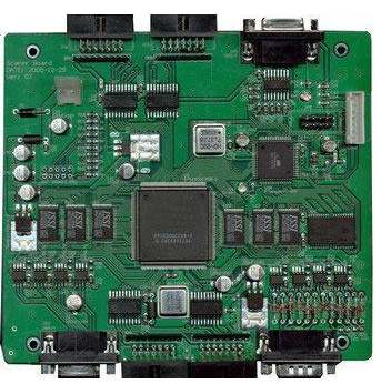
These PCB systems consist of slots containing redundant switch cards, line cards, and power modules. They can be equipped with redundant components to increase the reliability and availability of installation. Figure 1 shows a typical system configuration based on modular chassis. The backplane interface solution (also known as high-speed serial connection) provides full duplex communication between high-speed backplanes. The speed of the serial connection device depends on the system throughput requirements. The serial connection transmits data through high-speed differential signals. Then the differential signal is routed through the line card and connector, through the backplane and through another set of high-density connectors. Its channel characteristics depend on backplane material, connector density, routing width/coupling, etc. In a typical router, the routing length can be in the range of 1 inch to 48 inches, depending on where the line card is inserted into these routes.
The backplane interface devices in these modular chassis systems have the following key requirements:
1. Increase speed: interface devices shall meet the bandwidth requirements of system designers. Chip manufacturers are currently selling 3.125-5Gbps and providing samples of 6.25Gbps solutions to upgrade the solutions in the existing backplane. Through simple switch card upgrade, system manufacturers can reuse the existing chassis and line cards, and provide an upgrade path to higher bandwidth line cards to provide customers with more services at a low cost;
2. Backward compatibility: Backplane interface devices are required to work at the speed of the original line card to be compatible with the original line card;
3. High density and low power consumption: In order to cope with the increasing network traffic, these systems need smaller footprint, higher performance and density, and no additional power consumption. Therefore, there is always a demand for backplane devices with lower power consumption and faster speed.
4. Manufacturability and testability: The backplane interface device needs to integrate JTAG, BIST and other functions to achieve chip level and system level testing during prototype creation and manufacturing.
High speed backplane PCB design considerations
As the data rate exceeds the 1Gbps level, designers must solve new problems in their backplane system design. The signal integrity of these backplanes is affected by skin effect, dielectric loss, greater noise caused by crosstalk, and inter symbol interference (ISI).
Skin effect is a phenomenon, that is, with the increase of frequency, most of the current will concentrate on the external conductor. The loss caused by skin effect is proportional to the square root of frequency, the width and height of the cable.
The dielectric loss is caused by the dielectric heat loss of the plate, and it increases linearly with the frequency. At higher frequencies, dielectric loss becomes a more serious problem. These losses not only reduce the amplitude of the signal, but also slow down the edge speed of the signal, resulting in poor tolerance of signal divergence and jitter.
Because the low-frequency component with less attenuation is added to the high-frequency component with more attenuation on the receiver, signal divergence will lead to intersymbol interference. As a result, the eye map opening becomes smaller, so it is more difficult to recover on the receiving end, resulting in an unacceptable bit error rate. This limits the maximum bit rate. Another way to explain this phenomenon is that the signal "gets dirty" or diverges, causing the energy to drop bit by bit, thus causing bit error. At lower rates, ISI can be corrected because there is sufficient timing margin. However, at a higher rate, ISI is no longer limited to the signal boundary, but can affect the entire bit width.
The main source of noise is crosstalk caused by high-density connectors and backplane wiring. Crosstalk is a major noise source caused by high-density connector and backplane layout. There are two types of crosstalk: near end crosstalk (NEXT) and far end crosstalk (FEXT). NEXT will be caused when the signal from the transmitter close to the victim receiver interferes with the received signal. FEXT will be caused when the received signal is interfered by the "remote transmitter" connected to the victim receiver. All these channel damages can be compensated or eliminated by special signal adjustment (such as pre emphasis and equalization) circuits in backplane interconnection devices. These circuits compensate for signal loss by attenuating low-frequency components and amplifying high-frequency components.
Innovative signal adjustment technology
The key role of backplane interface devices is to solve the channel damage problems such as loss and crosstalk, and thus extend the service life of the backplane. The interface transmitter has signal adjustment circuits such as amplitude control and pre emphasis.
Similarly, the backplane interface receiver uses equalization technology to control the loss. In addition, these devices are required to have testable characteristics such as JTAG and BIST, so that they can be tested at the system level during manufacturing. National Semiconductor's four way 5Gbps SerDes can meet all these requirements. The following describes in detail the signal integrity technology used by the four way 5Gbps backplane transceiver SCAN50C400 pair and other high-speed backplane interface devices.
Pre emphasis and de emphasis: This PCB technology pre distorts the signal before transmission, so that the signal quality on the receiver is the same as that of the original transmission. When the signal remains at DC level for more than one bit, the pre emphasis will raise the high-frequency component and reduce the low-frequency component. In the process of designing these methods, PCB system designers must carefully control the output amplitude to limit the output power.
Receive equalization: Receive equalization compensates the loss characteristics of the channel by using the relative frequency characteristics of the input data. There are two types of equalization circuits: fixed and adaptive. The fixed equalizer manually sets the compensation characteristics, while the adaptive equalizer uses an adaptive algorithm to set the optimal compensation characteristics, which enables users to apply a device to various channels. It can also automatically compensate for changes in channel characteristics caused by manufacturing deviation and environmental changes.
The receive equalization function can be integrated into the backplane interface device or executed in an independent device. The advantage of performing receive equalization in a separate device is that it provides the best PCB routing advantage and design flexibility.
Learn PCB design skills for high-speed circuits
Jan 04,2023


Just upload Gerber files, BOM files and design files, and the KINGFORD team will provide a complete quotation within 24h.