
Professional PCB manufacturing and assembly
Building 6, Zone 3, Yuekang Road,Bao'an District, Shenzhen, China
+86-13410863085Mon.-Sat.08:00-20:00

PCB design passes aspect ratio: design, signal integrity and manufacturability
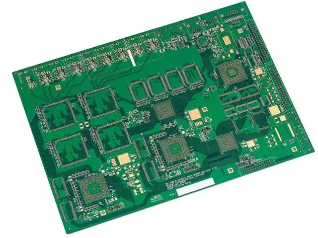
There is some beauty in nature, which can only be imitated in PCB design. The golden ratio found in nature is a good example of defining the general relationship between the aspect ratio of plants and animals. Like anything, a PCB board can have several layers: a conductive layer, a dielectric layer, a potential barrier layer, and a layer that comes with drilling. Although the aspect ratio of through-hole is not the golden ratio, they have a unique appearance and are extremely important in PCB design.
The aspect ratio of through-hole is a profound problem that many designers are willing to ignore. In short, the aspect ratio of a through-hole is its length divided by its diameter. Although it may seem subtle, aspect ratio of through-hole is important in various PCB applications. It is also important to consider the aspect ratio when considering manufacturing requirements.
How Through Hole Aspect Ratio Affects High Speed Plate Design
With the continuous improvement of digital signal transmission speed, any impedance discontinuity will affect the signal quality. The vias placed in signal lines are impedance discontinuities that are often ignored in PCB. Through holes may exhibit inductive and/or capacitive discontinuities, and these parasitic elements degrade signal quality as the signal passes through the through hole. Whether through characteristic impedance or noise reduction, signal integrity is a long-term challenge.
The impedance of the through-hole can be adjusted without using additional capacitors or inductors to compensate for the through-hole impedance. To compensate for parasitic capacitance in the aspect ratio vias, all non functional pads along the vias barrel must be removed. Capture pads should be as small in diameter as possible, which also helps maximize cabling space. In addition, using drill back to remove it by stubs can mitigate signal integrity issues. Any remaining through-hole pile will have inductive discontinuity and cause signal reflection when the signal passes through the through-hole.
Like differential traces, vias for high-speed signals can be designed in a differential manner. The signal through-hole can be placed side by side with the grounding circuit through-hole. The grounding and signal vias used for differential distribution lines must have the same geometry, including aspect ratio, to maintain symmetry and take full advantage of crosstalk reduction. The increase of grounding via can also improve insertion/return loss.
Drilling tolerance
When understanding your board requirements and PCB manufacturing material requirements, the thickness of the board is not the only problem on your board. Different manufacturers have different manufacturing capabilities. Most manufacturers should be able to place through holes in a width to height ratio of 6:1 to 10:1. The IPC reliability standard also specifies an aspect ratio of 6:1 to 8:1. An aspect ratio of 8:1 is considered necessary for PCB manufacturers.
Whether blind holes or buried holes are used, or holes are placed through mechanical drilling, the key parameter is the hole diameter rather than the length width ratio. Smaller diameters require tighter drilling tolerances. If the drill bit deviates slightly from the target, the drill bit can pierce the trace leading to the through hole, thus making the circuit board virtually useless, because its hole only misses its mark.
Laser drilling faces the same horizontal mechanical tolerance requirements as mechanical drilling. However, laser drilling facilitates the formation of smaller through holes without subjecting the plate to the stresses imposed during mechanical drilling. This process can greatly improve your PCB manufacturing and greatly change your electronic product production relationship.
The obtained aspect ratio is proportional to the focus depth divided by the beam waist, and the aspect ratio can be slightly controlled by controlling these two parameters. The use of lasers with smaller wavelengths, such as ultra fast UV lasers, can further reduce the via diameter and reduce the drilling time during manufacturing and manufacturing.
Through electroplating challenges
Drilling through holes will require some understanding of the complexities, including increasing the depth of the circuit and the need for increased manufacturing. The aspect ratio of through-hole will affect the difficulty of internal plating. Copper is deposited inside the through-hole using an electroplating solution. The plating solution must be able to be sucked into the through-hole through the capillary action core to completely plate the interior of the through-hole.
The physics and chemistry involved in microcolumn electroplating are very interesting. During capillarity, the surface tension draws the plating solution into the through-hole, and copper begins to deposit along the wall. Due to the meniscus formed on the solution surface, the copper precursor will be rapidly consumed from the solution in the deeper area of the through-hole. As a result, the inner part of the through hole barrel can have a thinner coating than the edge of the through hole.
If the aspect ratio of the through-hole is large, the copper coating inside the through-hole will be thinner, and the center of the through-hole will be easier to crack under thermal stress. The plating solution with lower viscosity can cover the interior of the through-hole with high aspect ratio more effectively. This not only improves the structural strength of the through-hole, but also improves the reliability of its thermal stress resistance.
The strength and reliability of through-hole vary from manufacturer to manufacturer. This can happen even though the through-hole has the same aspect ratio. Due to the weight of copper deposited in the through-hole and the thickness at the center caused by the electroplating method used in the manufacturing process, there will be a significant difference in reliability. PCB processing, PCB assembly and processing plants share PCB design through aspect ratio: design, signal integrity and manufacturability.


Just upload Gerber files, BOM files and design files, and the KINGFORD team will provide a complete quotation within 24h.