
Professional PCB manufacturing and assembly
Building 6, Zone 3, Yuekang Road,Bao'an District, Shenzhen, China
+86-13410863085Mon.-Sat.08:00-20:00

Ring and multilayer PCB design: keep within tolerance
Similarly, to make the multilayer PCB design work normally, it is necessary to complete the entire process. However, if there is no through-hole, they will be everywhere. The through-hole is essentially a vertical drilled shaft that bridges any number of gaps between layers.
However, even though vias need to be considered, otherwise your design may encounter failures. The annular ring works when considering the physical location of the hole through each through-hole trace. There are several factors to consider when determining the appropriate ring size for your application.
Ring connection strength: via and multilayer PCB
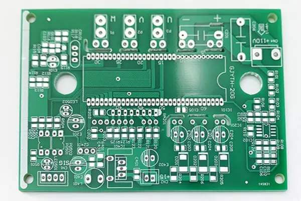
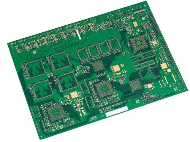
Because multilayer PCBs can handle higher complexity, they are beneficial to some printed circuit boards. Computers, telephones, and medical devices are some examples of applications that benefit from multi-layer design. However, when using multilayer PCBs, connecting these layers to each other presents a key problem. If you do not connect each layer to its corresponding point, you can only glue multiple single-layer PCBs to each other.
Input through hole; Our ingenious solution for vertically connecting each layer. However, the vias need to know the annular ring to work properly. These rings are defined as the minimum distance between the drilled hole and the through hole trace edge. The larger the ring, the more copper connections will be around the hole.
The use of rings usually determines the size you want to photograph. Are you soldering components to one side or both sides of the board? You may need a larger area for welding. Do you just use it as a test point without welding? The smaller ring size can help you.
No matter what application you use on the ring, you can easily determine the size with our trusted old friend IPC-7251. This document recommends a maximum material condition (MMC) of 250 µ m ring width. MMC just means that you will have the strongest solder joints. On the other hand, the recommended ring width is 150 µ m to achieve a minimum material state (LMC). LMC just means that you will get rid of the weakest solder joint connection. PCB assembly and PCB design factory explain the design of annular ring and multilayer PCB: keep within the tolerance range, annular connection strength: via and multilayer PCB.
Obviously, these are just suggestions and can (and should!) Make changes based on your specific application.
Manufacturing Tolerance of Multilayer PCB Design
When any combination of multiple manufacturing processes occurs in the production environment, because of the tolerance of defects here and there, some minor errors often occur, and these errors will overlap. Specifically, when the process of etching copper wiring on a PCB is combined with the process of drilling through holes through the wiring, your drilling will generally not be fully aligned in the center of these wiring, and will make you slightly deviate from the alignment. But don't be afraid. The tolerance is here!
Since you should already design for manufacturing tolerance errors, there is no difference in the design for circular tolerance tolerance. First, by determining the manufacturer's specific tolerance, they will be able to adapt to the error and determine the minimum width of the ring, which can safely reduce the risk of the entire manufacturing process and ensure that the minimum value is always reached.
In short, knowing that there will be some manufacturing errors along the way, but designing for these errors will make you higher than the minimum, especially for annular rings with drilled through holes.
Drilling tolerances can play an important role in determining the dimensions of your rings.
Calculate ring width
A simple way to verify that the width is acceptable for design is to calculate the maximum width that will be seen in post production. The following formula can be used:
((diameter of wire pad) - (diameter of drilling hole))/2=(maximum ring width)
The greater the manufacturing error of the tolerance, the smaller the width of the ring. The larger the diameter of the drill hole, the smaller the width of the annular ring.
Know that the width of your ring should be able to provide a strong enough connection for electrical and mechanical connection, and understand that manufacturing tolerance will keep your ring width at an acceptable distance, and there will be no drilling or even no contact with the hole. PCB assembly and PCB design factory explain the design of annular ring and multilayer PCB: keep within the tolerance range, annular connection strength: via and multilayer PCB.


Just upload Gerber files, BOM files and design files, and the KINGFORD team will provide a complete quotation within 24h.