
Professional PCB manufacturing and assembly
Building 6, Zone 3, Yuekang Road,Bao'an District, Shenzhen, China
+86-13410863085Mon.-Sat.08:00-20:00

The screen printing design process of the circuit board can generally be divided into two aspects, namely, screen drawing and screen drying. These two aspects have their own small differences. Let's go to have a detailed understanding of how the production process is.
1. Pull the net
Mesh pulling steps: mesh frame cleaning - horizontal calibration - coating adhesive layer - mesh pulling - tension measurement - coating adhesive - lowering the mesh and sealing the edge - storage
Specific operating instructions:
Due to the repeated use of the mesh frame, the residual viscose, screen yarn and other sundries around the mesh frame must be removed to avoid affecting the adhesion of the screen yarn and the mesh frame
Place the mesh frame on the platform (horizontal) to check whether the mesh frame is deformed. If it is deformed, it needs to be leveled
After cleaning, apply a thin and even layer of Nanbao weight grease (without adding hardener) on the joint surface between the undeformed screen frame and the screen yarn to enhance the adhesion between the screen yarn and the screen frame after stretching
After the first gluing for about 10 minutes, place the screen frame on the screen pulling table, and adjust the relative position and height
Select the mesh, loosen the clamping mouth around, lay the screen yarn on the frame, and then clip the screen yarn into the clamping mouth evenly without wrinkles. Note that there should be more loose screen yarn at the four corners, the clamping mouth must be locked, and there should be no gap between the clip and the clip (for example, automatic rack lifting and manual mesh pulling)
Wire drawing: the first tension is 26, and the tension is 24 after 5 minutes of standing; The second tension is 28, and the tension is 26 after standing for 5 minutes; The tension is 32 for the third time and 30 for 5 minutes; For the fourth time, the tension of 5 points shall be corrected to 32, and the gluing tension shall be 30 after standing for 20 minutes; The lower screen tension is 28 after 15 minutes of glue curing, and the screen plate can be made after standing for 72 hours (one meter × One meter automatic production line uses screen plate as an example).
Use a small brush to evenly brush the adjusted glue over the joint surface between the screen frame and the screen yarn. Do not drop the glue into the middle of the screen plate. After the glue dries for 8 minutes, use the scraper glue to press and paste the incomplete joint on the gluing surface for about 10 minutes. After the glue is completely dried (open air dryer should be used to strengthen the drying), it can be removed from the screen
Remove the excess screen yarn around the screen, and indicate on the screen frame the date, mesh and tension when lowering the screen (so as to observe the change of tension). In order to prevent the penetration of white water, seal the inner corner of the screen frame with red glue, and then seal it with waterproof tape above the joint surface of the screen frame and the screen yarn to prevent the penetration of liquid medicine
2. Net drying
Washing the screen: remove the grease (new screen) with the grinding paste, remove the graphics (old screen) with the ghost paste, remove the screen paste and blue oil with the desizing powder, wash the debris with the white water, wash the screen with the detergent, and finally wash it with the high-pressure water gun, and finally clean it with pure water.
Barbecue - The set temperature of the oven should be less than 48 ° C.
Sticker film: clean the net and then clean it with pure water. Select the water film according to the project film mosaic pattern by about 20%, press one end of the water film with a triangle ruler on the net, then slowly scrape it up with a triangle ruler, gently press it with a rubber spatula, and dry it with a towel
Use of stencil: dry the stencil and then apply the stencil. Use a scraper box to scrape the stencil box onto the stencil, including three times of green oil, (about once every 10 minutes or more) the bottom oil, and two times of top oil. Apply 50K water film on the blue glue first to tear off the film, and then apply the stencil 20 times, scraping three times each time (we have adopted an automatic sizing machine), and then dry the stencil after sizing.
Selection of screen yarn: 120T, 100T, 110T screen yarn for general line, green oil, base oil, top oil, 51T carbon oil, 24T blue glue photosensitive line and 77T heat curable green oil
18K water film is used for the selection of the film line (no screen paste is used, because the screen paste is uneven, which will produce dog teeth, fat oil and waves), screen paste is used for green oil, base oil and surface oil, and 50K water film is used for carbon oil
Paste the required engineering graphic film on the selected position of the screen and place it on the exposure machine for exposure. The time of exposure (3000W spotlight) is generally 60-80 seconds for lines, 80-100 seconds for green oil, 40-60 seconds for character oil on the bottom, 350-400 seconds for carbon oil and blue glue
Rinse the screen with pressurized water and dry it.
Seal the outside edge of the graphic film with blue oil (sealing paste) and dry it.
Check, repair the screen, write the completion date and corresponding number, and record and store.
Of course, this is just a general operation step. The ancients believed that it is better to have no books than to have no books. If we strictly follow this method in practical operation, it is extremely unwise. We should learn and use flexibly, so that we can make continuous progress and make better products.
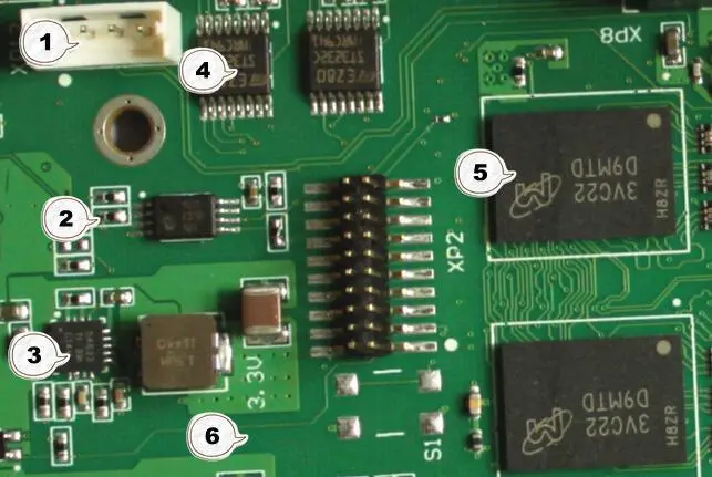
PCB silk screen specification
PCB screen printing technology has many specifications, which can not be done casually. These specifications have promoted the development of PCB screen printing technology. Let's take a look at the specifications:
All components, mounting holes and positioning holes have corresponding silk screen labels to facilitate the installation of finished boards. All components, mounting holes and positioning holes have corresponding silk screen labels. The silk screen of mounting holes on PCB is marked with H1, H2... Hn.
Silk screen characters shall follow the principle of from left to right and from bottom to top. Silk screen characters shall follow the principle of from left to right and from bottom to top as far as possible. For polar devices such as electrolytic capacitors and diodes, the direction shall be consistent in each functional unit as far as possible.
There is no silk screen on the device bonding pad and tin path that needs tin coating, and the device tag number should not be covered by the device after installation. (except for PCB with high density that does not need silk screen)
In order to ensure the welding reliability of components, it is required that there is no silk screen on the PCB component pad; In order to ensure the continuity of tin coating, it is required that there is no silk screen on the tin coating; In order to facilitate device insertion and maintenance, the device tag number shall not be covered by the device after installation; The silk screen shall not be pressed on the through hole and bonding pad to avoid the loss of part of the silk screen when the resistance welding window is opened, which will affect the training. The screen spacing is greater than 5mil.
The polarity of polar components is clearly shown on the silk screen diagram, and the polarity direction marks are easy to identify.
The number of PCB photo files is correct, each layer should have correct output, and a complete number of layers should be output.
The identifier of components on PCB must be consistent with that in BOM list.
The direction of the directional connector is clearly indicated on the silk screen.
The PCB shall be provided with barcode position identification. If the space on the PCB surface allows, the PCB shall be provided with 42 * 6 barcode silk screen frame. The position of the barcode shall be convenient for scanning.
The silk screen position of PCB name, date, version number and other information of the finished board shall be clear. PCB documents shall be printed with board name, date, version number and other board information, with clear and striking location.
PCB must have complete relevant information and anti-static identification of PCB manufacturer.


Just upload Gerber files, BOM files and design files, and the KINGFORD team will provide a complete quotation within 24h.