
Professional PCB manufacturing and assembly
Building 6, Zone 3, Yuekang Road,Bao'an District, Shenzhen, China
+86-13410863085Mon.-Sat.08:00-20:00

How to Solve Design Problems Early in PCB Design
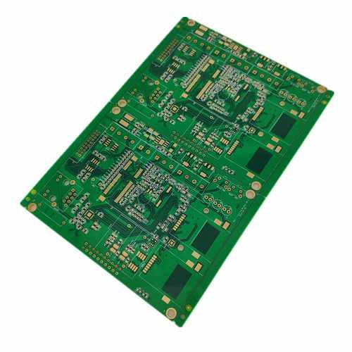
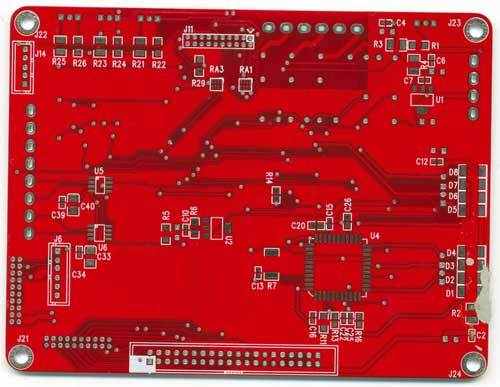
The design of printed circuit board is based on the circuit schematic diagram to realize the functions required by the circuit designer. The design of printed circuit board mainly refers to layout design, which needs to consider the layout of external connections. The optimal layout of internal electronic components, the optimal layout of metal wiring and through-hole, electromagnetic protection, heat dissipation and other factors. Excellent layout design can save production costs and achieve good circuit performance and heat dissipation. Simple layout design can be realized by hand, while complex layout design needs to be realized by computer aided design (CAD)
What measures have you taken to check the quality test of PCB boards to ensure that you do not have to worry about problems after production? The key is analysis automation. Read on to learn more.
"I am running PDN Analyzer on the board currently being manufactured ™, But I have discovered a mistake I made. My footprints are full of holes, but I forgot to make them into shutters, and they are devouring my powered aircraft. It proved to be a very useful tool to identify these problems before I got involved in manufacturing. "
Everyone is faced with the same nightmare. He wakes up on the other side of the news and learns that due to costly mistakes, the newly released products must be alleviated on the spot. Even worse, products that you now have to spend hours designing must be recalled.
These situations may have a negative chain reaction to the whole company. In this era of loud cries from consumers, it may even make you hate the theme tag, which can be seen by people all over the world. Considering this situation will make you wonder whether any measures can be taken to reduce the impact of on-site errors, or is it just the essence of the project when luck is not around you?
Traditional path of field disaster
You have just received the final results of the accelerated life test of the evaluation board. Everything looks good and it is ready for production. The premise of the life testing process is very simple - if your prototype equivalent to production passes the quality testing stage, you must have a reliable PCB, right? FALSE.
The fact is that it is impossible to test the long-term pressure that your PCB will bear in the field under various conditions and use cases. The products we design today have higher IC power consumption, which is mainly driven by density and speed. When you combine the demand for increasing density and speed with the reduced power demand, your distribution network becomes a complex voltage track maze, which will provide lower voltage as the current speed increases.
When you put this high current density mixture together, you may find:
PCB delamination and pinch point fusing.
The resistance of heat-resistant copper increases, resulting in a voltage drop.
Increasingly complex power management challenges due to thermal contributions.
It is not easy to deal with this complex maze, which can improve board density and speed and reduce power consumption. So what do you need to do to ensure that enough metal is provided on the board without relying on conservative rules of thumb and limited prototype simulations?
Understand changes before and not after production
The key to solve the field fault lies in the pcb design process itself, not later. If you can see what you look like when designing, and make necessary changes, then production will become the final benchmark, rather than a constantly changing finish line. Circuit board assembly and circuit board processing manufacturers explain how to solve design problems prematurely in circuit board design.


Just upload Gerber files, BOM files and design files, and the KINGFORD team will provide a complete quotation within 24h.