
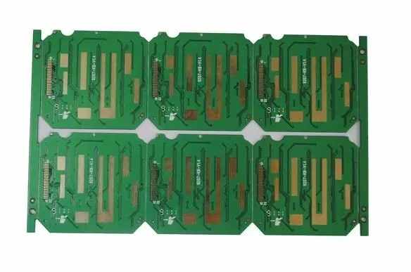
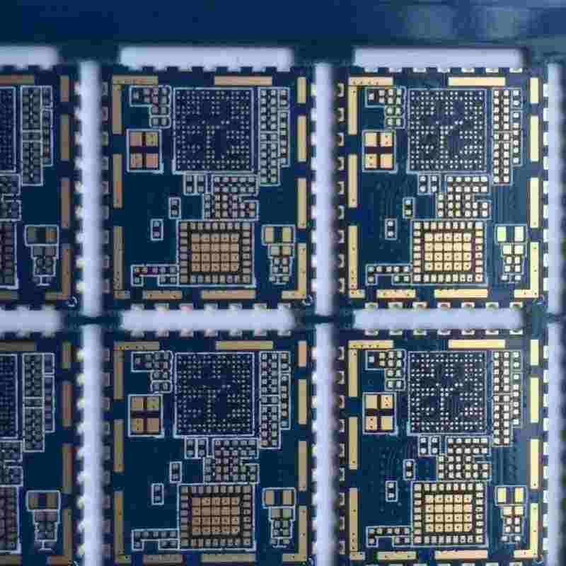
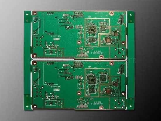
Professional PCB manufacturing and assembly
Building 6, Zone 3, Yuekang Road,Bao'an District, Shenzhen, China
+86-13410863085Mon.-Sat.08:00-20:00

Here are 8 PCB design and layout skills you should know
PCB is everywhere, and we may never be more than one meter away from PCB. Your smartwatch/fitness tracker, laptop or mobile phone. We can't rely on PCB somewhere one day! As a result, PCB design is more important than ever. In this article, we discussed some of the most important elements of successful PCB design, as well as the eight layout techniques you should know.
1. Node location is critical
Perhaps the most important tip on our list is node accessibility. This can help solve your design problems and solve them during testing. If the node is not accessible, testing becomes more difficult regardless of the type of node you use. If they are easy to detect, they are also easy to test.
2. Space issues
Today's circuit boards support more components per square centimeter than ever before. From the end user's perspective, this is great. The more components on the board, the more functions it supports, and the more times users can use the device for operations. However, for the end user, the advantage is the challenge to the designer.
In short, the more components are added to the board, the greater their limitations in the design. Furthermore, there is no doubt that element spacing is very important. Why is this? You will find several reasons. One of them is that without proper spacing, you will not have enough cabling space. Another challenge is that these components generate heat, and the closer the packaging is, the more heat will accumulate in the circuit board. In some cases, this may be enough to damage the plate material itself, especially if you are using materials such as FR-4, rather than materials designed to withstand high heat.
3. Feel hot
Heat will always be a problem, but not insurmountable. A quick tip to help you solve problems related to high temperatures is to add additional copper around surface mounted components. This will generate more surface area and help dissipate more heat faster, effectively turning part of the PCB design into a heat sink.
4. Pay attention to the arrangement
Sometimes, simply rotating parts is not enough. When this happens, it is important to take some strategies in component arrangement to deal with this situation. But what?
Cascade components: Cascade components play a crucial role in many PCB design options. However, they may be difficult to arrange correctly. Keep them close to each other and make sure they are in order on the board. This will immediately eliminate the challenge of trying to route the entire board to connect cascading components located in different areas.
Merge: Why use multiple smaller resistors when a higher resistor works better? Merging your design ensures that more space is left for components and routing, because resistors will take up less of your available space.
Cascade from edge: When layout PCB design, please determine all components that must be connected by connectors placed on or near the edge. Place these components as close to the connector as possible. The rest of the chain shall be cascaded from this point to form adjacent functional blocks.
5. Make room
Does the following sound familiar? You are looking at your PCB design, trying to fit each component into it and wire between them. No matter where they are placed, they will face many problems, especially when the circuit board is small.
answer? Rotate the components and find the best layout so that you can route directly between them while maximizing the space on the entire board. This may take some time and effort, but it is worth the least investment.
6. The feeling of contraction
Struggle on a circuit board that cannot be routed? Use smaller components. By using a smaller footprint, you will leave more space for copper wiring through each component. Smaller components are also easier to maintain proper spacing, which helps you avoid board overcrowding and other problems caused by stacking components too close to each other.
What should you do? Although square flatpack components may be your first choice, you may need to consider using ball grid array components. Of course, there are trade-offs here – smaller components make maintenance more challenging.
7. Dense plate
If you are working hard on PCB design, the space required for wiring, vias and gaps is likely to become a problem. You can solve this problem by being more intensive. With HDI, you can create very dense circuit boards with very dense routing, gaps, and vias, which still provide performance. However, when designing for high current and high voltage, you really need to consider the controlled impedance wiring, differential pairs, and check the creepage distance, gap and width.
8. Reduce noise
When some routing is involved, signal noise may become a problem. However, placing wires carrying high-frequency signals too close will couple these signals, increasing noise and possibly causing problems on wires that do not require noise. Make sure you keep noisy digital cabling away from analog cabling to avoid this problem. The circuit board assembly and circuit board processing manufacturers explain the 8 PCB design and layout skills that you should know. Now I will explain them to you.


Just upload Gerber files, BOM files and design files, and the KINGFORD team will provide a complete quotation within 24h.