
Professional PCB manufacturing and assembly
Building 6, Zone 3, Yuekang Road,Bao'an District, Shenzhen, China
+86-13410863085Mon.-Sat.08:00-20:00


Select the appropriate routing width for your next PCB design
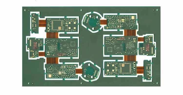
The design of printed circuit board is based on the circuit schematic diagram to realize the functions required by the circuit designer. The design of printed circuit board mainly refers to layout design, which needs to consider the layout of external connections. The optimal layout of internal electronic components, the optimal layout of metal wiring and through-hole, electromagnetic protection, heat dissipation and other factors. Excellent layout design can save production costs and achieve good circuit performance and heat dissipation. Simple layout design can be realized by hand, while complex layout design needs to be realized by computer aided design (CAD)
Another factor to consider when designing single-layer and multilayer PCBs is the wiring width. Like other design factors of PCB, the requirements for good wiring width may affect the layout and size of PCB. Reducing PCB size can reduce costs, but you still need to ensure that you have enough space to accommodate the effective routing width.
Why is routing width important?
The effective wiring width ensures that the wiring (whether signal wiring or power wiring) operates effectively and provides the best PCB functions.
Top 5 Precautions
PCB wiring width can be determined after considering the following factors:
Purpose: power supply wiring or signal wiring?
Amperage: or, current, through the trace.
Location: top or bottom layer, or inner layer, the heat cannot escape as soon as possible.
Thickness: How thick is the copper on the layer?
Length: How long is the wiring?
Standard Practices
Width – Typically, the width of the wire used to transmit the signal can be less than the width of the wire used to transmit the current. For current optimized routing, a good range of widths may vary from 0.010 inch for 0.3 amperes to 0.150 inch for 6.0 amperes.
Shape – The trace can be arranged on the PCB layer horizontally or vertically or at an angle (45 degrees). For trace widths of 0.012 inch or less, right angle or acute corner turns are not recommended. Try to make the routing as short and direct as possible. If you use traces along the edge of a layer, make sure there is enough space between the trace and the edge of the layer, usually 10 to 15 mils.
Spacing – The traces are too close to each other or other components, which may lead to the risk that the circuit board may be short circuited during operation. 0.003 "can be the minimum distance between lines; The recommended spacing for most routing widths should be at least 0.010 inch. The spacing of higher voltage wiring shall be larger. The circuit board assembly and the circuit board processing manufacturer explain how to select the appropriate wiring width for your next PCB design.


Just upload Gerber files, BOM files and design files, and the KINGFORD team will provide a complete quotation within 24h.