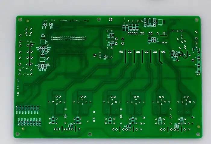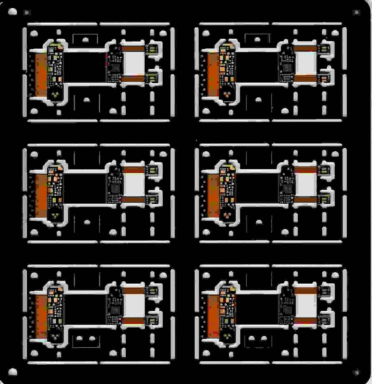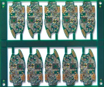
Do you know the PCB design under vacuum environment?
The columnist "Getting rid of the inherent manufacturing thinking mode" has been engaged in CAM engineering for decades, and he has also served as a PCB designer, so he has unique views on PCB design under the "vacuum environment". As he said, designers are not the only party isolated in the "vacuum environment" in this process.
Q: When designing PCB, do you not know which factory will manufacture and/or assemble the design?
A: It depends on the complexity of the project. For example, if the design needs to consider the controlled impedance, the line width, line spacing and medium required to achieve the impedance should be negotiated with the manufacturer before the design and layout; If there are special requirements, the design engineer should even visit the factory in person to ensure that he understands the complexity of the operation. Many companies will have a design engineer or field application engineer prequalify the manufacturer to ensure that the factory can complete the order and review the required details.
I heard that if PCB manufacturing is difficult, designers will stay in the factory throughout. In addition, it is very helpful to establish a solid relationship between designers and factory engineers. If the designer and manufacturing engineer cooperate for the first time, when the manufacturing engineer has questions about the design, he will usually call the contact person (usually the project manager or procurement personnel), and then contact the designer. The manufacturing engineer who can raise questions is an essential part of the entire production process.

However, the designer may not know who will manufacture or assemble in the future. For example, the selected manufacturer may have a long delivery time or other unpredictable complications, and have to be delivered to another manufacturer for production. Note: In this case, if the controlled impedance is required in the design, let the new manufacturer review whether there will be large routing or spacing changes, and decide whether to redesign, including widening the routing when the allowable small spacing limit has been designed.
Other obstacles may also lead to a complete redesign, such as choosing different material types (due to supply chain problems), which greatly increases the workload of designers. If you really want to ensure production, you must communicate clearly.
Q: Why do so many designers not know who will manufacture PCB designed by them in the future?
A: One reason is the company culture. If the purchasing department of the designer's company does not share information about the component manufacturer, the designer must ask exploratory questions. I think there is no reason for purchasing personnel to intentionally conceal the information of selected manufacturers, but this situation still exists.
Remember, cost is proportional to product quality. If the factory lacks quality control and an operation needs to be redesigned many times, it will not only lose time. I believe that companies with comprehensive management will always share information with the designers and engineers of the project, especially the specific projects related to the success of components should be passed on to manufacturers.
Another possible reason is also related to the company's procurement culture. They don't care where the parts are manufactured, as long as the results meet expectations and the cost and delivery time meet requirements. In my opinion, this will lead to many problems and may lead to misunderstanding of expectations and results. For designers, a "simple" PCB may not be that simple for the manufacturer that produces it.
Q: What information or data will be missing?
Answer: PCB design is a hierarchical structure. As a designer, you should start from a known point and ask questions about the unknown that can be foreseen at the first customer meeting. Start by reviewing the schematic to determine power and component placement.
Designers may have more problems. When it comes to power, designers often raise issues related to power management ICs. When talking about PMIC, one of my former bosses said, "I have done such a case that I can track the reference and input very closely. I think it can achieve the requirements very well, but it still requires some hard work to achieve the goal correctly. In crowded areas, it is usually not easy to add or move capacitors and try to squeeze more copper or through-hole areas."
It is not humiliating to ask questions, but we should try to catch as many questions as possible in each question and solve them. Customers don't like endless questions. More importantly, they don't want to waste time on these additional questions.
Things that can be "designed" are unnecessary, such as solder mask color or impedance calculation, which need to be completed during layout. At the same time, the assembly placement is completed before the layout. All phases of the design work should be checked and balanced, such as a review of component placement by the end user.
The above is my introduction to "PCB design under vacuum environment" for your reference. Do you know PCB design under "PCB design, introduction of PCB manufacturers to vacuum environment"? PCB design under the "vacuum environment" has a unique point of view.


