
Professional PCB manufacturing and assembly
Building 6, Zone 3, Yuekang Road,Bao'an District, Shenzhen, China
+86-13410863085Mon.-Sat.08:00-20:00

PCB design process, the whole process of PCB design products
Know how to design printed circuit boards. PCB is a key element in any electronic circuit design process. The layout and design of PCB have a great impact on the working mode of the circuit. Therefore, if the PCB design is effective, the circuit will be executed more reliably within its specification range.
1、 Pcb design environment
For commercial development schemes, there may be CAD and CAD software packages, which are required due to complexity. Even for students and amateurs, there are many very good bags, whether free, which can be obtained at a moderate cost. Free software provides basic functions, while high-end software packages enable more facilities to be included in the design: analog circuits, complex circuits, multilayer circuits, etc. With the increase of the speed of digital boards and the RF design reaching higher and higher frequencies, the ability to simulate is becoming a higher and higher requirement.
2、 Circuit schematic diagram
The first stage of PCB design and development is the schematic design of the circuit, which can be realized in various ways. Some pcb design software comes with schematic drawing. We import the schematic file into the pcb design tool to generate a "Netlist". The grid table connects each pin, connected devices and circuit nodes together.
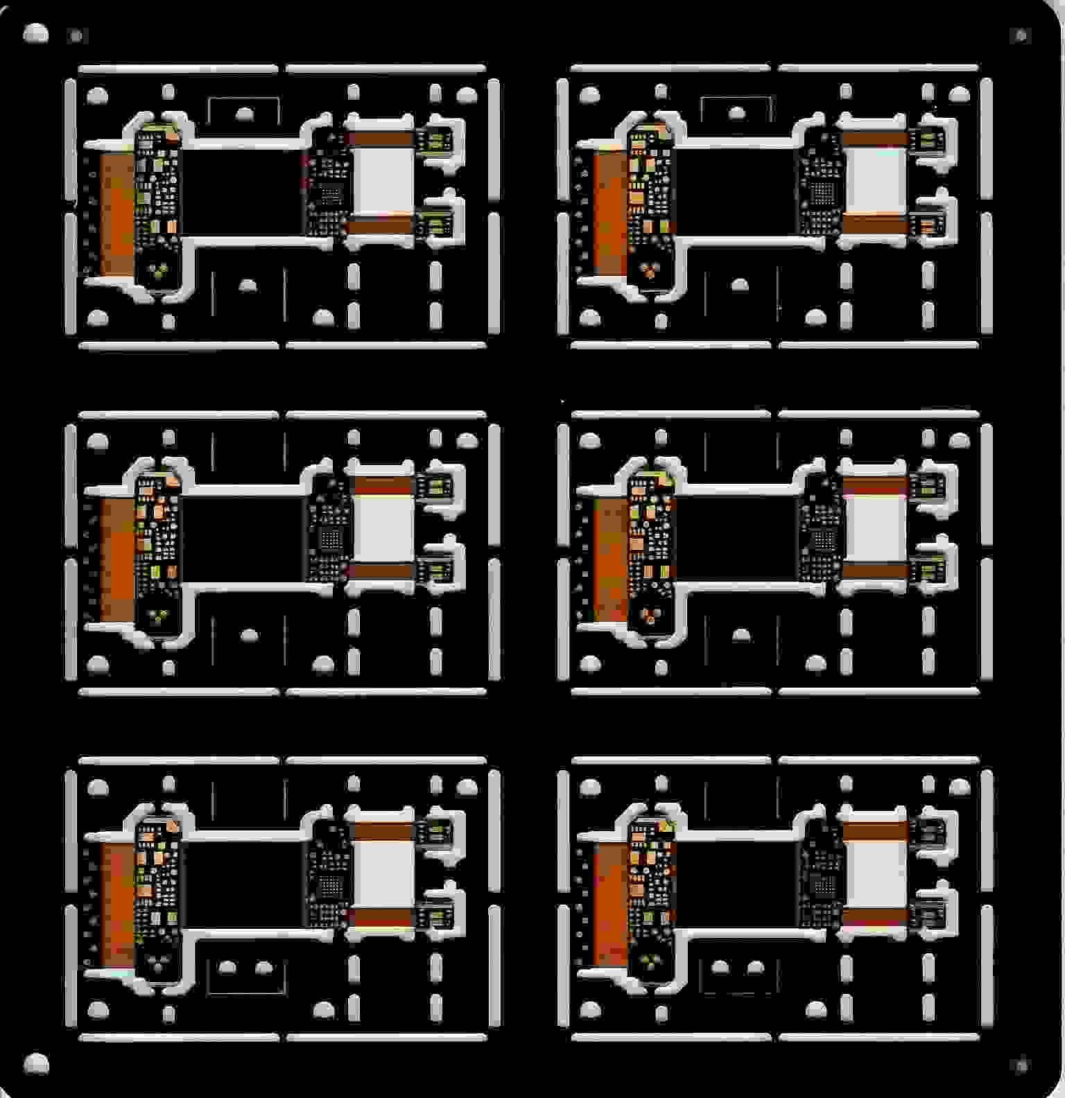
3、 Pcb component initialization
Before detailed PCB design and layout, it is necessary to roughly understand where the components will be located and whether there is enough space on the board to contain all the required circuits. This will enable people to determine the number of layers required for the circuit board and whether there is enough space to contain all the circuits that may need to be carried out. Once the space and approximate position of components are roughly estimated, more detailed component layout can be provided for PCB design. This can take into account aspects such as the proximity of devices that may need to communicate with each other, and other information related to any RF considerations. In order to enable the components to be included in PCB design, they must understand all relevant information of the components, including the shape of the circuit board, aperture information, far away area, and so on. In general, several devices may share the same pin, so it is not necessary to enter this information for each component part number. Create a package library for all devices in PCB design. In this way, previously used components can be easily called.
4、 Wiring
Once the basic components are placed, the next stage of PCB design is to route the connections between all components. Then, PCB software routes according to the information in the Netlist table in the schematic diagram. In order to achieve this, it will use the number of layers available for the connection, created by holes as needed. Generally, one layer will be allocated as GND layer and the other layer will be allocated as power supply plane. This not only reduces the noise level, but also makes the power of the low source resistor connection. Cabling is time-consuming, especially for large designs with more than 3000 or 4000 components. When cabling becomes difficult due to the density of multiple components, this may result in a large amount of time spent on cabling.
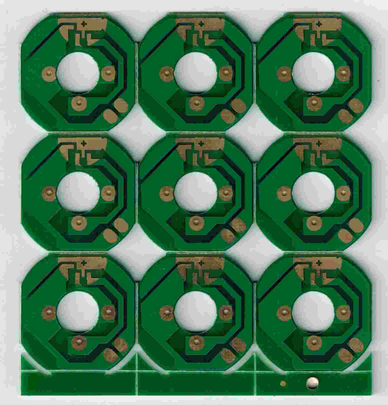
5、 Pcb file (gerber)
Output the photo map information of PCB layout in the form of Gerber file. This format is the standard for PCB files, and they are in the form of NC files used by photo plotters. In addition to Gerber files, drilling information and screen printing and photo saving information are also generated. A major factor in PCB costs is drilling. In any design, some holes are required for fixing, as well as holes required for conventional parts. However, in order to reduce costs, it is advisable to use as few hole sizes as possible. In this way, the bit will require less variation and time can be reduced.
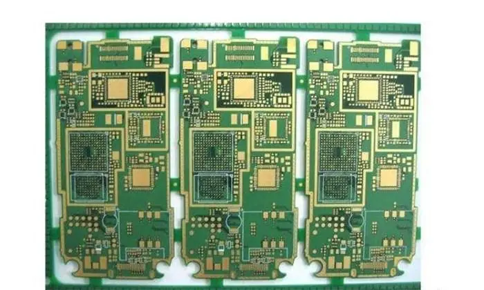
PCB files are used in many areas of the manufacturing process. It is not only used for the manufacturing of PCB itself, but also these documents will be used in other areas of the manufacturing process. Such as making steel mesh, SMT patch, ICT test, pin test home, etc. The above is the whole process of PCB design products. PCB design is not just drawing design. Introduction to PCB assembly and PCB processing manufacturers: explanation of the whole process of PCB design products.


Just upload Gerber files, BOM files and design files, and the KINGFORD team will provide a complete quotation within 24h.