
Professional PCB manufacturing and assembly
Building 6, Zone 3, Yuekang Road,Bao'an District, Shenzhen, China
+86-13410863085Mon.-Sat.08:00-20:00

High frequency pcb board wiring design skills: 1. The shorter the lead between the pins of the high frequency circuit board components, the better; 2. The less the lead bends between the pins of the high-speed PCB components, the better; 3. The ground wire of the high frequency digital signal and the ground wire of the analog signal are isolated; 4. Avoid walking
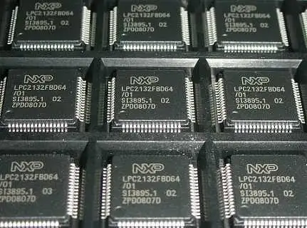
High frequency circuit board
1、 The shorter the lead between pins of high-frequency circuit board components, the better
The radiation intensity of the signal is proportional to the routing length of the signal line. The longer the high-frequency signal lead is, the easier it is to be coupled to the PCB components close to it. Therefore, for high-frequency signal lines such as the signal clock, crystal oscillator, DDR data, LVDS line, USB line, HDMI line and so on, the shorter the routing is, the better.
2、 The lead between pins of high-speed electronic devices should be bent as little as possible
The lead wire of high-frequency PCB wiring should preferably be a straight line, which needs to be turned. A 45 degree broken line or arc turn can be used. This requirement is only used to improve the fixation strength of copper foil in low-frequency circuits, while in high-frequency circuit boards, meeting this requirement can reduce the external transmission and mutual coupling of high-frequency signals.
3、 The ground wire of high-frequency digital signal is isolated from the ground wire of analog signal
When connecting analog ground wire, digital ground wire, etc. to the public ground wire, connect them with high-frequency choke magnetic beads or directly isolate them and select a suitable place for single point interconnection. The ground potential of the ground wire of high-frequency digital signals is generally inconsistent, and there is often a certain voltage difference between the two. In addition, the ground wire of high-frequency digital signals often contains rich harmonic components of high-frequency signals. When the digital signal ground wire and analog signal ground wire are directly connected, the harmonic of high-frequency signals will interfere with the analog signal through the way of ground wire coupling. Therefore, in general, the ground wire of high-frequency digital signal and the ground wire of analog signal should be isolated, and the method of single point interconnection at a suitable location or high-frequency choke magnetic bead interconnection can be adopted.
4、 Avoid loops formed by routing
The routing of various high-frequency signals shall not form a loop as far as possible. If it is unavoidable, the loop area shall be as small as possible.
5、 The less lead layer alternation between pins of high-frequency circuit board components, the better
The so-called "less interlaminar alternation of leads, the better" means that the less vias (Via) used in the component connection process, the better. One via can bring about 0.5pF distributed capacitance. Reducing the number of vias can significantly improve the speed and reduce the possibility of data errors.
6、 A high-frequency decoupling capacitor is added to the power supply pin of the integrated circuit block. A high-frequency decoupling capacitor is added to the power supply pin of each integrated circuit block nearby. The high-frequency decoupling capacitor of the power supply pin can effectively suppress the interference caused by high-frequency harmonics on the power supply pin.


Just upload Gerber files, BOM files and design files, and the KINGFORD team will provide a complete quotation within 24h.