
Professional PCB manufacturing and assembly
Building 6, Zone 3, Yuekang Road,Bao'an District, Shenzhen, China
+86-13410863085Mon.-Sat.08:00-20:00

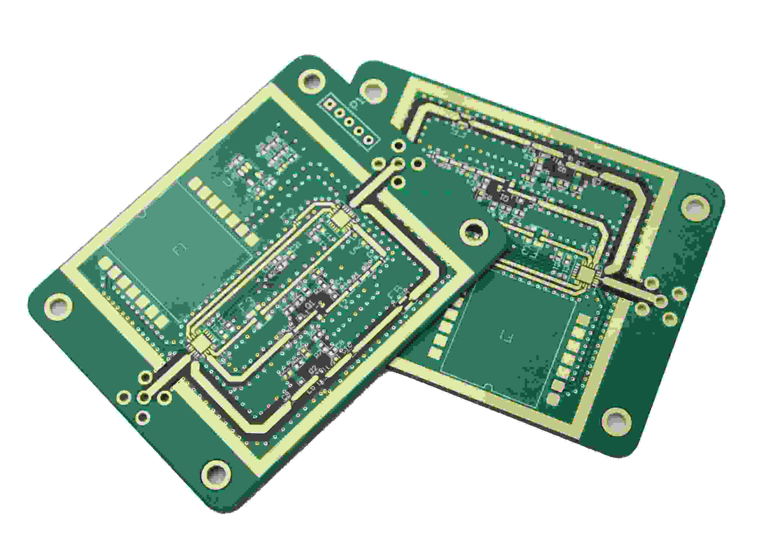
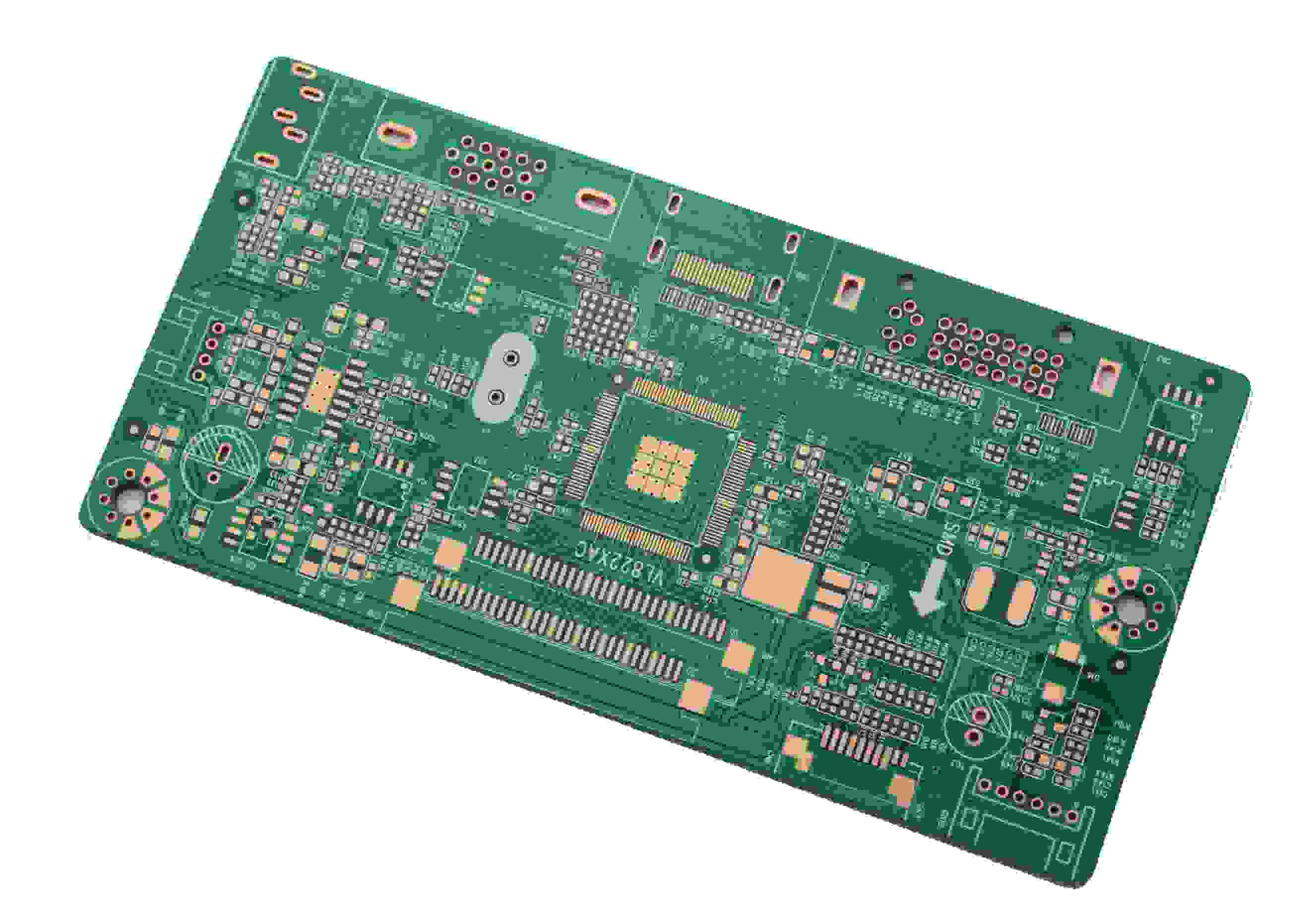
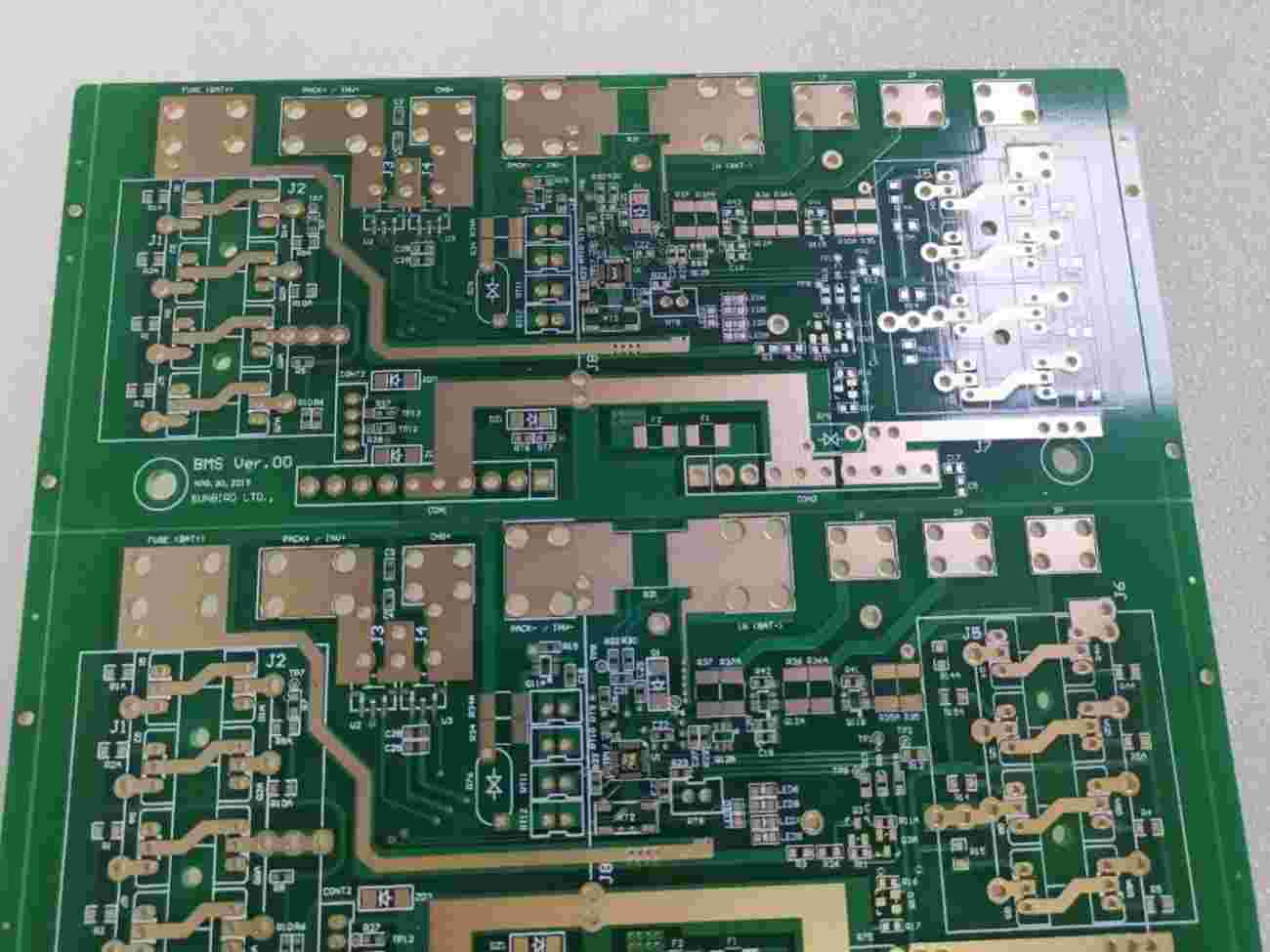
An example of pcb wiring technology in electronic factory
The design of mixed signal circuit PCB is very complex. The layout and wiring of components and the processing of power lines and ground wires will directly affect the circuit performance and EMC performance. This paper will introduce the division design of digital and analog circuits to optimize the performance of mixed signal circuits.
In PCB, to reduce mutual interference between digital signals and analog signals, two basic principles of electromagnetic compatibility (EMC) must be understood before design:
·Minimize the area of the current loop;
·The system uses only one reference plane.
If there are two reference planes in the system, a dipole antenna may be formed. If the signal cannot return through the smallest loop as possible, it may form a large loop antenna, which should be avoided as much as possible in the design.
Separate the digital ground and analog ground on the mixed signal circuit board, so as to realize the isolation between the digital ground and analog ground. Although this method is feasible, there are also many potential problems in this method, especially in complex large-scale systems. The most critical problem is that the wiring cannot cross the division gap. Once the wiring crosses the division gap, electromagnetic radiation and signal crosstalk will increase dramatically. The most common problem in PCB design is the EMI problem caused by the signal line crossing the partition ground or power line.
1. Division method 1
If division mode 1 is adopted, and the signal line crosses the gap between two grounds, what is the return path of the signal current? It is assumed that the two divided grounds are connected at some place (usually at a single point at a certain position). In this case, the ground current will form a large loop, and the high-frequency current flowing through the large loop will generate radiation and high inductance.
If the low level analog current flows through the large loop, the current is easily interfered by external signals. When the split ground is connected together at the power supply, a very large current loop will be formed. In addition, analog ground and digital ground are connected to the ˉ It will form a dipole antenna.
Understanding the path and mode of current return to ground is the key to optimize the mixed signal circuit board design. Many designs only consider where the signal current flows, ignoring the specific path of the current. If the ground wire layer must be divided and must be routed through the gap between the divisions, a single point connection can be made between the divided ground to form a connection bridge between the two grounds, and then the wiring can be routed through the connection bridge. In this way, a direct current return path can be provided below each signal line, so that the formed loop area is very small.
The optical isolation device or transformer can also be used to realize the signal crossing the separation gap. For the former, it is the optical signal that spans the segmentation gap; For the latter, it is the magnetic field that crosses the gap. Another feasible method is to use differential signal: the signal flows in from one line and returns from another signal line. In this case, the ground does not need to be used as the return path.
2. Division method 2
In practical work, PCB is generally divided into analog part and digital part. Analog signals are routed in the analog area of all layers of the circuit board, while digital signals are routed in the digital circuit area. In this case, the digital signal return current will not flow to the ground of the analog signal.
Only when the digital signal is wired on the analog part of the circuit board or the analog signal is wired on the digital part of the circuit board, will the digital signal interfere with the analog signal. This kind of problem does not occur because there is no division. The real reason is that the wiring of digital signals is inappropriate.
PCB board design adopts a unified approach. Through digital circuit and analog circuit zoning and appropriate signal wiring, it can usually solve some more complex layout and wiring problems, but also will not produce some potential troubles caused by ground segmentation. In this case, the layout and partition of components become the key to determine the design quality.
If the layout and wiring are reasonable, the digital ground current will be limited to the digital part of the circuit board and will not interfere with the analog signal. Such wiring must be carefully checked and checked to ensure compliance with the wiring rules, otherwise, improper routing of a signal wire will completely destroy the design of a circuit board.
3. A/D partition
When connecting the analog ground and digital ground pins of the A/D converter, most A/D converter manufacturers will recommend that AGND and DGND pins be connected to the same low impedance ground through the shortest lead, because most A/D converter chips do not connect analog ground and digital ground together internally, and the connection between analog ground and digital ground must be realized through external pins, Any external impedance connected to the DGND will couple more digital noise to the analog circuit inside the IC through the parasitic capacitance. According to this suggestion, it is necessary to connect the AGND and DGND pins of the A/D converter to the analog ground.
If the system has only one A/D converter, the above problems can be easily solved. Divide the ground and connect the analog ground and digital ground under the A/D converter.
If there are many A/D converters in the system, if the analog ground and digital ground are connected together under each A/D converter, the multipoint connection will be generated, and the isolation between analog ground and digital ground will be meaningless. If not, the manufacturer's requirements will be violated.
The best way is to uniformly divide the analog part and digital part at the beginning.
Such layout and wiring not only meet the requirements of IC device manufacturers for low impedance connection of analog and digital ground pins, but also do not form a loop antenna or dipole antenna. Pcb design, pcb manufacturers introduce pcb design pcb wiring technology examples.


Just upload Gerber files, BOM files and design files, and the KINGFORD team will provide a complete quotation within 24h.