
Professional PCB manufacturing and assembly
Building 6, Zone 3, Yuekang Road,Bao'an District, Shenzhen, China
+86-13410863085Mon.-Sat.08:00-20:00

How to set pcb board routing rules for pcb board designers
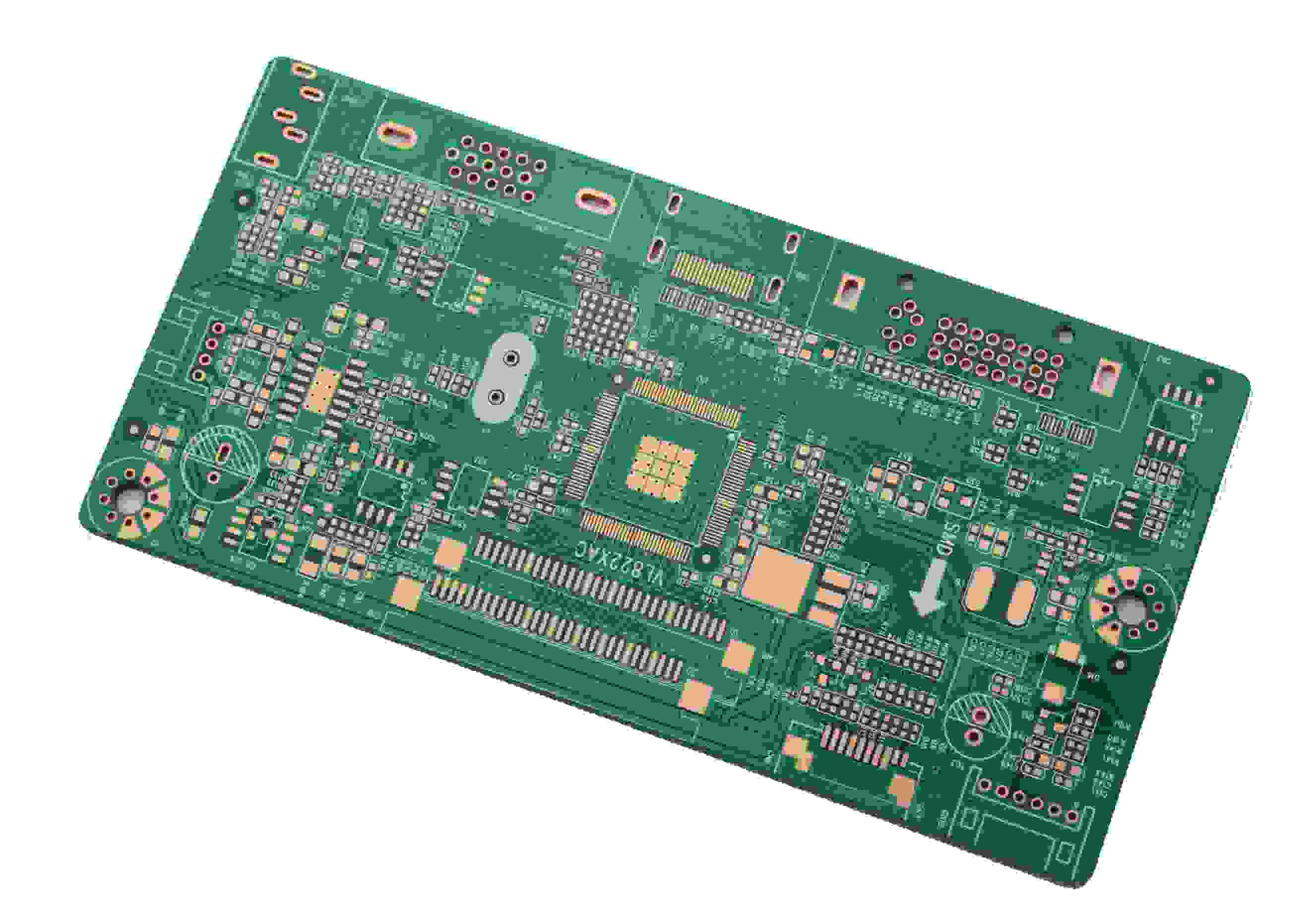
The design of printed circuit board is based on the circuit schematic diagram to realize the functions required by the circuit designer. The design of printed circuit board mainly refers to layout design, which needs to consider the layout of external connections. The optimal layout of internal electronic components, the optimal layout of metal wiring and through-hole, electromagnetic protection, heat dissipation and other factors. Excellent layout design can save production costs and achieve good circuit performance and heat dissipation. Simple layout design can be realized by hand, while complex layout design needs to be realized by computer aided design (CAD)
Before routing, you should generally set the routing rules. The general settings are as follows. Take the settings in Prote1 as an example to briefly introduce.
(1) Safety clearance setting.
The safety clearance setting corresponds to the Clearance Constraint item in Routing, which specifies the distance that must be kept between the routing, pads and vias of different networks on the PCB. The safety distance of general PCB can be set as 0.254mm, the empty PCB can be set as 0.3mm, and the dense patch PCB can be set as 0.2~0.22mm.
(2) Setting of routing layer and direction.
The routing layer and direction correspond to the Routing Layers item in Routing, where you can set the used routing layer and the main routing direction of each layer. Please note that the single-sided PCB board of the patch only uses the top layer, and the in-line single-sided PCB board only uses the bottom layer, but the power layer of the multi-layer PCB board is not set here.
(3) Setting of via shape.
The vias shape corresponds to the Routing Via Style item in Routing, which specifies the minimum, maximum and preferred values of the inner and outer diameters of vias automatically generated during manual and automatic routing, of which the preferred value is the most important.
(4) Setting of routing lineweight.
The routing line width corresponds to the Width Constraint item in Routing, which specifies the width of routing in manual and automatic wiring. The preferred item in the whole PCB range is 0.2~0.6mm. In addition, the line width settings of some networks or network groups Net Class, such as ground wire, AC power input wire, power output wire, and power group, can be defined in Design NetlistManager in advance. The ground wire is generally 1mm wide, and various power lines are generally 0.5~1mm wide. The circuit board assembly and processing manufacturers introduce how circuit board designers set pcb circuit board routing rules.


Just upload Gerber files, BOM files and design files, and the KINGFORD team will provide a complete quotation within 24h.