
Professional PCB manufacturing and assembly
Building 6, Zone 3, Yuekang Road,Bao'an District, Shenzhen, China
+86-13410863085Mon.-Sat.08:00-20:00

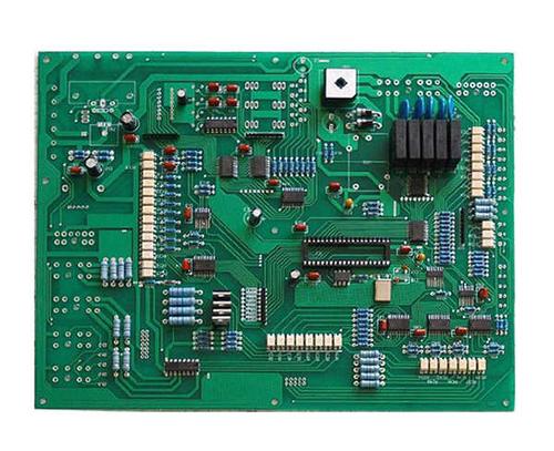
PCB wiring process requirements: ① In general, the signal line width is 0.3mm (12mil), and the power line width is 0.77mm (30mil) or 1.27mm (50mil); The distance between lines and between lines and pads shall be no less than 0.33mm (13mil). In practical application, if conditions permit, it shall be considered
PCB wiring process requirements:
①. Line
In general, the signal line width is 0.3mm (12mil), and the power line width is 0.77mm (30mil) or 1.27mm (50mil); The distance between lines and between lines and pads shall be greater than or equal to 0.33mm (13mil). In practical application, if conditions permit, the distance shall be increased; When the wiring density is high, it can be considered (but not recommended) to use two lines between IC pins, the width of the line is 0.254mm (10mil), and the line spacing is not less than 0.254mm (10mil).
Under special circumstances, when the device pins are dense and the width is narrow, the line width and line spacing can be appropriately reduced.
②. Pads
The basic requirements for PAD and VIA are: the diameter of PAD is greater than that of hole by 0.6 mm; For example, universal pin resistors, capacitors and integrated PCB circuits adopt 1.6mm/0.8mm (63mil/32mil) disk/hole dimensions, 1.8mm/1.0mm (71mil/39mil) sockets, pins and diodes 1N4007, etc. In practical application, it shall be determined according to the size of the actual component. If possible, the pad size can be appropriately increased; The component installation hole diameter designed on the PCB shall be 0.2~0.4mm larger than the actual size of the component pin.
③. Via (VIA)
Generally 1.27mm/0.7mm (50mil/28mil); When the PCB wiring density is high, the via size can be appropriately reduced, but should not be too small, and 1.0mm/0.6mm (40mil/24mil) can be considered.
④. Spacing requirements for pads, wires and vias
PADandVIA:≥0.3mm(12mil)
PADandPAD:≥0.3mm(12mil)
PADandTRACK:≥0.3mm(12mil)
TRACKandTRACK:≥0.3mm(12mil)
When the density is high:
PADandVIA:≥0.254mm(10mil)
PADandPAD:≥0.254mm(10mil)
PADandTRACK:≥0.254mm(10mil)
TRACKandTRACK:≥0.254mm(10mil)
Fifth: wiring optimization and silk screen printing. "There is no best, only better"! No matter how hard you try to design, after you finish painting, you will still feel that there are many places that can be modified. The general design experience is that the time for optimizing the routing is twice as long as the time for the first PCB routing. I don't think there is anything that needs to be modified. After that, I can lay copper (Place ->polygonPlane). Copper is generally laid with ground wire (pay attention to the separation of analog ground and digital ground), and power supply may also be required for multi-layer boards. For silk screen, it should be noted that it cannot be blocked by devices or removed by vias and PCB pads. At the same time, when designing, face up to the component surface, and the characters at the bottom layer should be mirrored to avoid confusing the layers.
Sixth: Network and DRC inspection and structure inspection. First, on the premise of confirming that the circuit schematic design is correct, NETCHECK the generated PCB network file and the schematic network file for the physical connection relationship, and correct the design in time according to the output file results to ensure the correctness of the wiring connection relationship; After the network check is passed correctly, DRC check shall be carried out on the PCB design, and the design shall be corrected in time according to the output file results to ensure the electrical performance of PCB wiring. Finally, the mechanical installation structure of PCB needs to be further checked and confirmed.
Seventh: Plate making. Before that, it is better to have an audit process. PCB design is a mental work. The PCB board designed by the person who is thoughtful and experienced is good. Therefore, we should be extremely careful in design, fully consider all factors (for example, many people do not consider the convenience of maintenance and inspection), and strive for perfection, so that we can design a good board.


Just upload Gerber files, BOM files and design files, and the KINGFORD team will provide a complete quotation within 24h.