
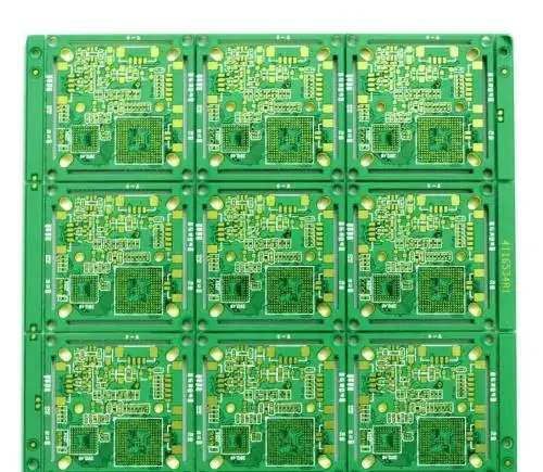
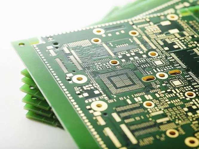
Professional PCB manufacturing and assembly
Building 6, Zone 3, Yuekang Road,Bao'an District, Shenzhen, China
+86-13410863085Mon.-Sat.08:00-20:00

PCB design Gerber layer setting and silk screen specification in PCB design
Circuit board assembly and circuit board processing manufacturers explain the Gerber layer setting of circuit board design and the silk screen specification in circuit board design
1. The layers to be output are:
(1) Wiring layer includes top/bottom/intermediate wiring layer;
(2). The power layer includes VCC layer and GND layer;
(3) Resistance welding layer includes top resistance welding and bottom resistance welding;
(4). The silk screen layer includes the top/bottom silk screen;
(5) In addition, the drilling file NCDrill should be generated.
2. Select Board Outline when setting the Layer of each layer.
3. If the power supply layer is set to Split/Mixed, select Routing in the Document item of the Add Document window and use the Plane Connect of PourManager to copper coat the PCB before outputting photo files each time; If it is set to CAMPlane, select Plane. When setting the Layer item, you need to add Layer25 and select Pads and Vias in Layer25.
4. In the device setting window, press Device Setup to change the Aperture value to 199.
5. When setting the layer of the silk screen layer, do not select Part Type. Select the Outline Text Line of the top and bottom layers and the silk screen layer.
6. When setting the layer of the solder mask layer, selecting via means that there is no solder mask on the via, and not selecting via means that there is solder mask depending on the specific situation.
7. Do not change the default settings of PowerPCB when generating drilling files.
8. After all photo files are output, open them with CAM350 and print them. The designer and reviewer will check them according to the "PCB checklist".
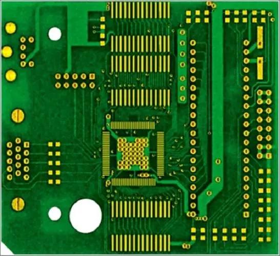
Silk screen specification in PCB design
1. The polarity of polar components is clearly indicated on the silk screen diagram, and the polarity direction marks are easy to identify.
2. The direction of directional connectors is clearly indicated on the silk screen.
3. All components, mounting holes and positioning holes have corresponding silk screen labels. To facilitate the installation of the finished board, all components, mounting holes and positioning holes have corresponding silk screen labels. The silk screen of the mounting holes on the PCB is identified by H1, H2... Hn.
4. The silk screen characters shall follow the principle of from left to right and from bottom to top. The silk screen characters shall follow the principle of from left to right and from bottom to top as far as possible, and the polarity devices such as electrolytic capacitors and diodes shall be kept in the same direction in each functional unit as far as possible.
5. There is no silk screen on the device bonding pad and tin path that needs tin coating, and the device tag number should not be covered by the device after installation. (except for those with high density and without silk screen on PCB)
In order to ensure the welding reliability of devices, it is required that there is no silk screen on the device bonding pad; In order to ensure the continuity of tin coating, it is required that there is no silk screen on the tin coating; In order to facilitate device insertion and maintenance, the device tag number shall not be covered by the device after installation; The silk screen shall not be pressed on the through hole and bonding pad to avoid the loss of part of the silk screen when the resistance welding window is opened, which will affect the training. The screen spacing is greater than 5mil.
6. The PCB shall be provided with barcode position identification. If the space on the PCB surface allows, the PCB shall be provided with 42 * 6 barcode silk screen frame. The position of the barcode shall be convenient for scanning.
7. The silk screen position of PCB name, date, version number and other information on the finished board shall be clear. PCB documents shall be printed with board name, date, version number and other board information, with clear and striking location.
8. The identifier of components on PCB must be consistent with that in BOM list.
9. The PCB shall have complete relevant information and anti-static identification of the manufacturer.
PCB assembly and PCB processing manufacturers explain the Gerber layer setting of PCB design and the silk screen specification in PCB design.


Just upload Gerber files, BOM files and design files, and the KINGFORD team will provide a complete quotation within 24h.