
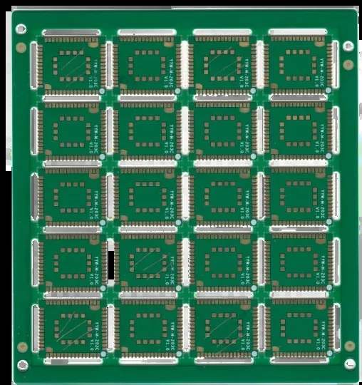
Professional PCB manufacturing and assembly
Building 6, Zone 3, Yuekang Road,Bao'an District, Shenzhen, China
+86-13410863085Mon.-Sat.08:00-20:00

PCB power wiring and switching power supply design PCB layout
PCB power wiring precautions and switching power supply must follow the high-frequency circuit wiring principle when designing PCB layout
Reasonable power line routing can prevent circuit from harmful coupling through power supply, which plays an important role in restraining interference. Pay attention to the following points when wiring:
(1) For the internal power supply of each unit circuit, the direction of power supply from the previous stage to the previous stage shall be adopted, and the filter capacitor of this unit shall be arranged near the last stage. If the stage with large working current of some circuits is not the last stage, the filter electrolytic capacitor can be set on the stage with large current. The power supply shall be laid forward and backward from this stage.
(2) The wiring between each board and the main power supply shall be conducted separately as far as possible, and it is not suitable to use a main power supply wire to distribute the wiring board by board.
(3) The total ground of the power supply refers to the connection between the power supply and the circuit load ground, which can only be a point. The location of the general grounding shall be reasonable, and the AC pulsating current shall not flow through the DC and sampling circuits in the regulated power supply.
(4) The power supply wiring in the board can adopt multi-channel power distribution according to the distribution of circuits in the board, which is the same as the requirements of ground wire shunting.
(5) When multi-level series decoupling circuit is used in the power supply, the direction of the power supply shall be arranged according to the sequence of series connection. Do not change the series sequence or change it to multi-stage parallel decoupling at will.
(6) For some main current parts, there should be a test gap on the printed wire, which should be sealed with solder at ordinary times, and opened with a soldering iron during measurement.
The switching power supply must follow the principle of high frequency circuit wiring when designing PCB layout
Switching power supply works in high frequency and high pulse state, which belongs to a special kind of analog circuit. PCB layout must follow the principle of high frequency circuit wiring.
1. Layout: The impulse voltage wiring shall be as short as possible, including the wiring from the input switch tube to the transformer and the wiring from the output transformer to the rectifier tube. The pulse current loop shall be as small as possible, such as the positive input filter capacitance to the negative return capacitance from the transformer to the switch tube. The X capacitor in the circuit from the output transformer end to the rectifier tube to the output inductor to the output capacitor return transformer should be as close to the input end of the switching power supply as possible. The input line should not be parallel to other circuits and should be avoided. The Y capacitor shall be placed at the enclosure grounding terminal or FG connection terminal. The common touch electric induction shall be kept at a certain distance from the transformer to avoid magnetic coupling. If it is not easy to handle, a shield can be added between the common inductance and the transformer. The above items have a great impact on the EMC performance of the switching power supply.
Generally, two output capacitors, one close to the rectifier tube and the other close to the output terminal, can affect the output ripple index of the power supply. The parallel connection effect of two small capacity capacitors should be better than that of one large capacity capacitor. The heating device shall be kept at a certain distance from the electrolytic capacitor to extend the service life of the whole machine. The electrolytic capacitor is the key to the service life of the switching power supply. For example, the transformer, power tube, high-power resistor shall be kept at a distance from the electrolysis. The space between electrolysis must also be reserved for heat dissipation. If conditions permit, it can be placed at the air inlet.
Attention shall be paid to the control part: the connection of the high impedance weak signal circuit shall be as short as possible, such as the sampling feedback loop, and the interference of the current sampling signal circuit, especially the current control circuit, shall be avoided during processing. Some unexpected accidents may occur if the processing is not easy. PCB assembly, PCB design, PCB processing manufacturers explain PCB power wiring and switching power design PCB layout.


Just upload Gerber files, BOM files and design files, and the KINGFORD team will provide a complete quotation within 24h.