
Professional PCB manufacturing and assembly
Building 6, Zone 3, Yuekang Road,Bao'an District, Shenzhen, China
+86-13410863085Mon.-Sat.08:00-20:00

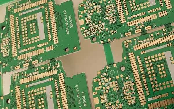
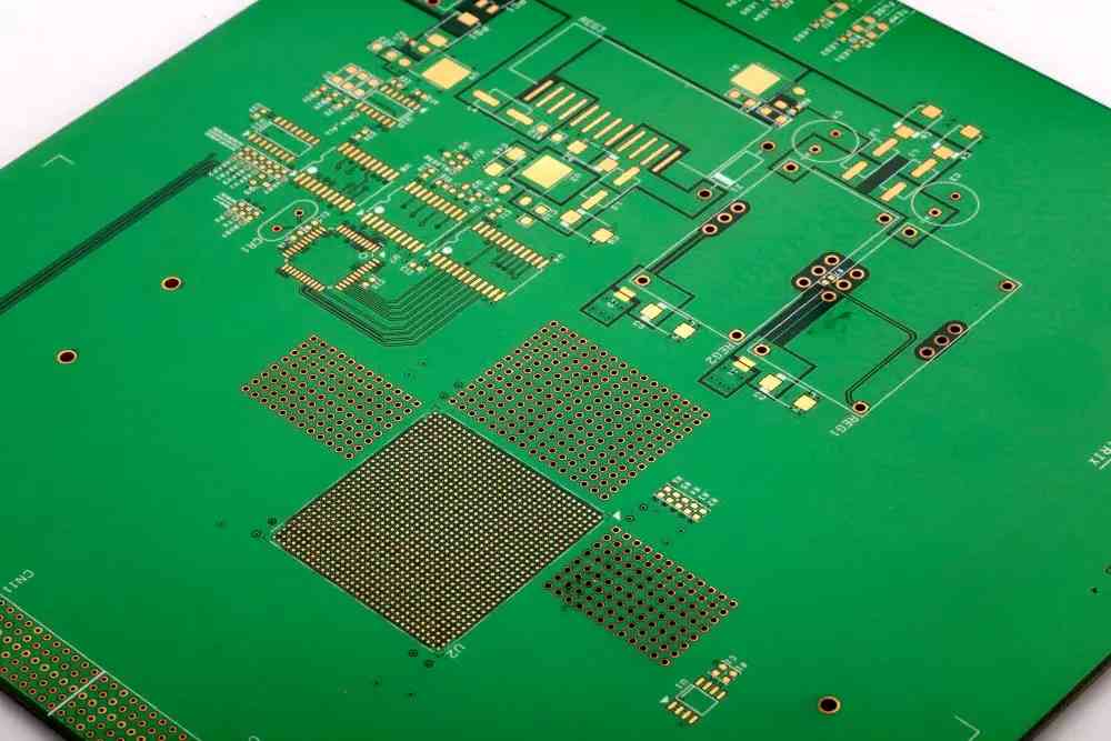
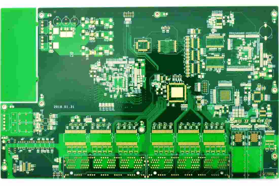
Six important PCB design specifications and PCB file conversion
1. Thermal pad. For some power devices, including power amplifier, power supply DCDC, PMU, etc., most of them are QFN or similar packages. In consideration of heat dissipation, there will be heat dissipation pads at the bottom of IC. However, when designing the engineer's pcb, it is necessary to open a piece of exposed copper on the top and bttom layers of the PCB, and connect it with a through hole in this area, so as to maximize the dissipation of heat energy as soon as possible. Because in the actual product design, heat dissipation is becoming more and more important.
2. The width of the power line is basically understood by engineers, but not described much. It can be estimated roughly by wiring or drawing copper sheet, basically following the formula of 40 mil bearing capacity 1A. Generally, it is better to reserve 25% redundancy.
3. Pin1 indicator. It is often known that when packaging chips, the position of pin1 is marked with triangle or circle symbols. However, it is often overlooked that this logo should be placed outside the chip package, so that the placement process can be completed. The factory production line can also detect errors during visual inspection. If the identification is inside, once the placement is completed, no problem can be found through visual inspection. The same problem applies to polar devices such as LEDs, diodes, tantalum capacitors, etc.
4. For the design with shielding frame, it should be noted that some RCL devices should not be too close to the position of shielding frame. It is easy to cause the problem of tin connection, especially some power networks. At the same time, the device should not be too close to the board edge.
5. For LCD or other FPC connectors, the pad length is at least 1mm longer than the actual pin pin length, mainly to increase the stability. In many drop tests, problems often occur here.
6. Similarly, for LCD connector, it is not recommended to place any components in the 3mm area around the connector.
Benefits of converting PCB files to drill data and GERBER files
Directly converting PCB files to drilling data and GERBER files will save a lot of trouble. While many electronic engineers will not convert PCB files to drilling data and GERBER files before submitting them to the factory when transferring PCB files to the factory, they are used to designing PCB files or exporting them from PCB board writing software and directly sending them to the PCB processing factory.
Because electronic engineers and PCB engineers have different understandings of PCB, the GERBER file converted from PCB factory may not be what you want. For example, when you define the parameters of components in PCB file during design, you do not want these parameters to be displayed on the finished PCB. You did not say that the PCB factory followed the lead and left these parameters on the finished PCB. This is just an example. If you convert PCB files to GERBER files yourself, you can avoid such events.
GERBER file is an international standard photo format file, which includes RS-274-D and RS-274-X formats. RS-274-D is called the basic GERBER format, and a D code file must be attached at the same time to fully describe a drawing; RS-274-X is called extended GERBER format, which contains D-code information. Common CAD software can generate these two formats.
How to check the correctness of the generated GERBER? You only need to import these GERBER files and D code files in the free software Viewmate V6.3 to see them on the screen or print them out through the printer.
Drilling data can also be generated by various CAD software, generally in Excel format, and can also be displayed in Viewmate. No PCB can be made without drilling data. The circuit board manufacturer explained six important PCB design specifications and the advantages of converting PCB files into drilling data and GERBER files.


Just upload Gerber files, BOM files and design files, and the KINGFORD team will provide a complete quotation within 24h.