
Professional PCB manufacturing and assembly
Building 6, Zone 3, Yuekang Road,Bao'an District, Shenzhen, China
+86-13410863085Mon.-Sat.08:00-20:00

Analysis of the Essential Conditions for PCB Layout to Become a Master
A prerequisite for a Layout master!
1 Tools and skill software: Allegro, WG and EN must know one of them. The work efficiency of these tools is much higher than Protel and PADS. Experts cannot waste a lot of time on tools. In addition, only those who use these tools will often do simulation. Hyperlynx can also do simulation with PADS sketchpad, but few people do this, such as our moderator Yang. In actual drawing, I have hardly seen anyone drawing boards with more than 20 layers using PADS, but there are many using Allegro and WG. Only those who often do simulation can have the theoretical basis of high-speed circuit board design.
Those who have not done simulation only know theory are mostly on paper. In addition to mastering one of the above tools, Protel, PADS and even ZUKEN also need to know something about the general characteristics of these tools and the file format, be able to convert common EDA file formats, and understand the packaging library design. Be able to check Gerber files with conventional CAM tools. In addition, you must master at least one impedance calculation tool, be familiar with the operating system, and be able to install and configure common EDA software. Be able to understand mechanical drawings in mainstream CAD format. Skillfully use the rule parameter constraint design, have designed single and double sided PCB boards and more than 10 layers of PCB boards, no less than 5 PCB boards with more than 10000 pins, no less than 10 PCB boards with more than 5000 pins, and no less than two years of pure layout experience.
Hardware: I have simply operated common instruments and tools, such as multimeter, soldering iron, oscilloscope, signal generator, etc., which can help hardware engineers to conduct simple board debugging and simply locate PCB related pcb layout design problems.
2 Theoretical basis: Be familiar with analog and digital electronics, be able to analyze simple circuit diagrams, basically understand the design ideas of hardware engineers, and be familiar with the high-frequency characteristics of common passive small devices. Be familiar with transmission line principle, bus, topology, timing, impedance matching and other basic concepts, be able to analyze the characteristics of common topology structures, and provide layout schemes for common multi load buses. Be familiar with the common parameters of signal quality, understand the mechanism of up and down rush, ringing, etc., and be able to preliminarily evaluate the advantages and disadvantages of eye pictures. Understand the basic principle of electromagnetic compatibility, and know the common types of electromagnetic compatibility certification.
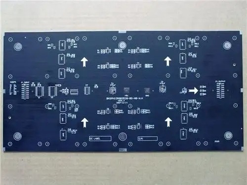
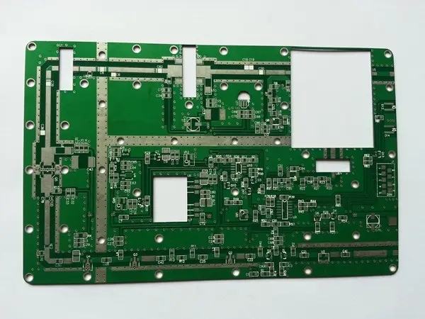
3 Process knowledge: understand PCB manufacturing process, familiar with common plates and their dielectric constant characteristics, know common plate surface heat treatment methods, understand the sequence of main manufacturing processes such as lamination, drilling, electroplating, and understand common manufacturing methods such as golden finger, grooving, bare grooving, and splicing. Understand the SMT production process, understand the characteristics of wave soldering and reflow soldering, and know several common component assembly methods and assembly sequence. Be able to formulate main layout process design rules according to the plate making process and SMT assembly process.
4 Language: Have the ability to read and write English, can understand more than 80% of Hi Speed Digital Design with the help of translation tools, and can basically understand foreigners' technical speeches.
5 Personal quality: good sense of teamwork, able to work together with other colleagues to successfully design highly difficult PCB. Lead a team or group with no less than 5 people, and be able to train new employees. The circuit board assembly and circuit board processing manufacturer explained that the circuit board layout must be analyzed to become a master.
How to debug a newly designed circuit board
Dec 02,2022


Just upload Gerber files, BOM files and design files, and the KINGFORD team will provide a complete quotation within 24h.