
Professional PCB manufacturing and assembly
Building 6, Zone 3, Yuekang Road,Bao'an District, Shenzhen, China
+86-13410863085Mon.-Sat.08:00-20:00

Circuit board factory explains the electronic and mechanical design of PCB
For a long time, we have a consensus that the manufacturing industry will naturally migrate to the country with the lowest cost, while the developed countries will suffer losses in this process. However, another point of view is that by outsourcing repeatable work, resources previously engaged in low value work will face greater opportunities. The same is true of design. By using design automation tools, engineers can improve their design efficiency. It is hard to imagine that today's engineers will not use computer methods to design PCB boards, although sometimes they can do so.
Just as the economy has to adapt to changes in global conditions, we encourage engineering teams to use any efficient design tool. For electronic design engineers, using EDA tools can greatly improve the design process, from components to final products. With the acceleration of the design process, we can now simulate or simulate every detail of electronic design before purchasing any component. For example, in the field of integrated circuit development, the final step of the long-term, high cost design process is to submit the design or 'trial production' as a silicon chip. The step of manufacturing integrated circuit will cost a lot, and this cost can be recovered only when the integrated circuit is sold in large quantities in the future. Of course, not all electronic product R&D is the same. The engineering cost of repeated manufacturing of most electronic products may be low, but for mechanical design, the gap between the shell and the internal PCB board will lead to the re manufacturing, which will require high costs.
The progress made in EDA tools means that it is easier to simulate the composition and function of products before they are manufactured. Even so, unlike IC design, the development of design automation tools in the field of electronic products used to focus on niche markets for specific applications. PCB design tools are an example. There are many low-cost PCB design tools that can be used to design simple, single-sided or double-sided boards, but there are few tools that can handle high-speed signals and mixed signals for multi-layer PCBs, and it is rare to provide PCB board tools that can perfectly solve signal integrity problems.
For the design with these needs, design tools are crucial. They provide the only feasible solution to help us live today's digital life. For example, without sophisticated EDA tools, it is impossible to achieve mobile communication; The tool helps talented engineers develop complex mixed signal equipment and systems required for 3G networks and smart phones.
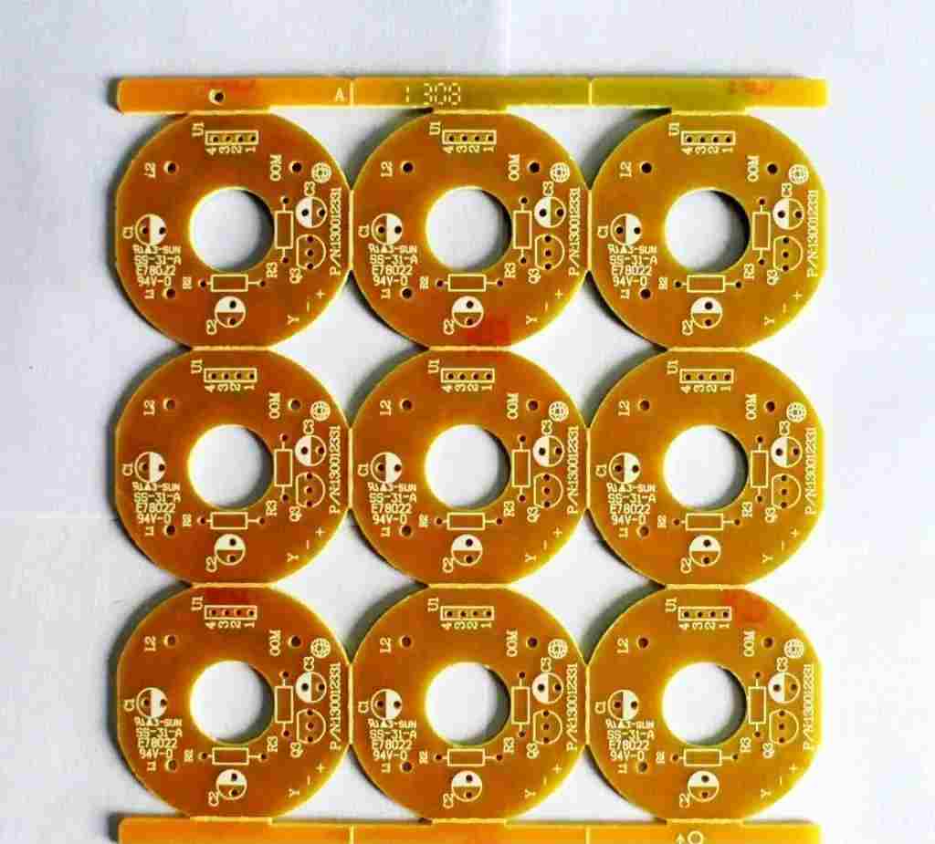
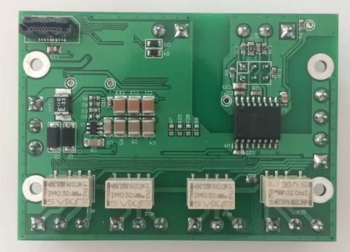
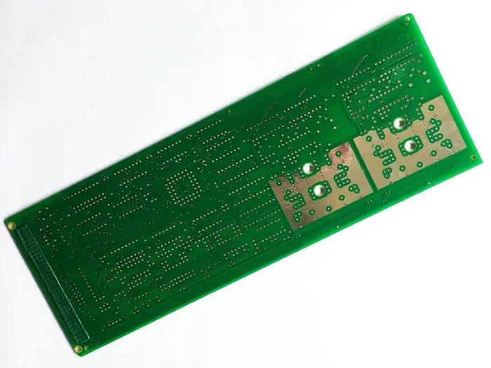
There are many related examples, but the basic trend can be summarized as follows: the more complex the design, the more sophisticated the tool needs. However, design tools are always used to develop products, regardless of the functional complexity or final market value of the product. PCB assembly, PCB design, and PCB processing manufacturers explain the electronic and mechanical design of PCB.


Just upload Gerber files, BOM files and design files, and the KINGFORD team will provide a complete quotation within 24h.