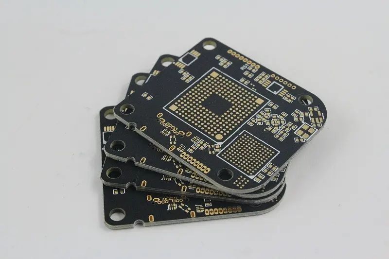
PCB factory engineers explain DDR PCB layout rules in detail
In the wiring of ordinary printed circuit boards, since the signal is a low-speed signal, it is generally OK to connect it according to the flow direction of the signal under the basic wiring rules of the 3W principle. But if the signal speed is above 100M, the wiring is very particular. Since the DDR signal with a speed of up to 300M has been distributed recently, please explain the wiring principles and techniques of DDR signal carefully.
High speed systems generally use low-voltage signals with low voltage and small swing, which is easy to improve speed and reduce power consumption, but this brings difficulties to the wiring. Because the low-voltage signal power is greatly affected by the internal resistance of the signal line, which is the relationship between the voltage and the square, the internal resistance should be reduced as much as possible, such as using electrical planes, punching more holes, shortening the wiring distance, and using resistors to separate the lower voltage signals at the end of high-voltage transmission. SDRAM, DDR-I, DDR-II and DDR-III signal voltages are lower than each other, which makes it more and more difficult to stabilize. The power supply should also be noted that if the power supply is insufficient, the memory will not work stably. The concept of signal integrity and transmission line is a highly professional system knowledge, which will not be described in detail here. Even if you don't understand the concept of signal integrity and transmission line, please follow the general basic rules below. The DDR high-speed signal board will not have problems.

1) The DDR and the main control chip shall be as close as possible. All differential signal pairs in the DDR high-speed signal shall be strictly equal in length (50 mils redundancy is allowed at most). The length of all signal lines and clock lines shall not exceed 2500 mils, and zero through-hole shall be allowed as far as possible. There must be a well grounded stratum below the element layer, and all the routing must not cross the ground dividing groove, that is, the stratum dividing line crossing the signal line cannot be seen from the perspective of the element layer. In this way, the 400M DDR is basically OK. Other 3W and 20H rules can be implemented as far as possible.
2) Address and command signal group: keep complete ground and power plane. The characteristic impedance is controlled at 50~60 Ω. The distance between the signal group and other non DDR signals shall be at least 20 mils. The intra group signal should match the length of the DDR clock line, with a gap of at least 500 mils. The RS value of the series matching resistance is O~33 Ω, and the RT value of the parallel matching resistance should be 25~68 Ω. The signals in this group shall not be in the same resistance bank as the data signal group.
3) Control signal group: the control signal group has the least signals, only clock enable and chip select signals. A complete ground plane and power plane are still required for reference. The RS value of the series matching resistance is O~33 Ω, and the RT value of the parallel matching terminal resistance is 25~68 Ω. In order to prevent crosstalk, signals in this group cannot be in the same resistance bank as data signals.
4) Data signal group: take the ground plane as a reference to provide a complete ground plane for the signal circuit. The characteristic impedance is controlled at 50~60 Ω. The line width is consistent with the clock signal width. At least 20 mils apart from other non DDR signals. The length matching is set by byte channel. The length difference of data signal DQ, data strobe DQS and data mask signal DM in each byte channel should be controlled within ± 100mil (very important), and the length difference of signals in different byte channels should be controlled within 500mil. The RS value of the series matching resistance of the matched DM and DQS is 0 ~ 33 Ω, and the RT value of the parallel matching terminal resistance is 25 ~ 68 Ω. If the resistor bank is used for matching, there should be no other DDR signals in the data resistor bank.
5) Clock signal: with the ground plane as the reference, provide a complete ground plane for the routing of the whole clock loop, and provide a low impedance path for the loop current. As it is a differential clock signal, the line width and line spacing shall be designed in advance before wiring, and the differential impedance requirements of CPU shall be understood before wiring according to this constraint. All DDR differential clock signals must be routed on the key plane to avoid layer to layer conversion. The line width and differential spacing shall ensure the principle of 3W. The single line impedance of the signal line shall be controlled at 50~60 Ω, and the differential impedance shall be controlled at 100~120 Ω. The distance between clock signal and other signals shall be kept above 20 mil * to prevent interference with other signals. The spacing of serpentine wiring shall not be less than 20 mils. RS value of series terminal resistance is 15~33 Ω, and RT value of optional parallel terminal resistance is 25~68 Ω. (The termination resistance shall be connected when the schematic diagram is designed)
6) In the power supply part, the decoupling capacitor should be placed near the power pin of the chip. The power supply and ground shall have independent layers for the return of signals with low resistance nearby. The power supply and stratum shall be drilled as many holes as possible to ensure good and smooth electrical connectivity.
As long as the above rules and techniques are followed, there will be no problem with the DDR high-speed signal from LAYOUT. In the equal length processing of each signal, in order to ensure the allowable error of the signal line length, the detour path processing can be used on purpose. Generally, the serpentine line is used for routing. We often see "equal length wiring". In fact, equal length is not the purpose, but the real purpose is to meet the establishment and holding time, the same frequency and phase, and correct sampling. Equal length is only the simplest way to achieve this goal, which requires quantitative analysis of line length. In terms of online characteristic impedance control, the thickness of the line should generally be required, but the manufacturing process and dielectric constant of each board manufacturer are different, so the board manufacturer should be required to control the characteristic impedance of the signal line. The circuit board assembly, circuit board design, and circuit board processing manufacturers introduce the circuit board factory engineers to explain the DDR PCB Layout rules in detail.


