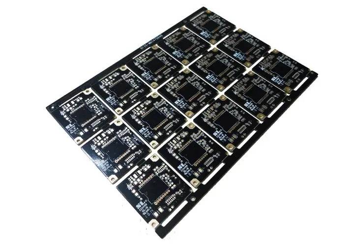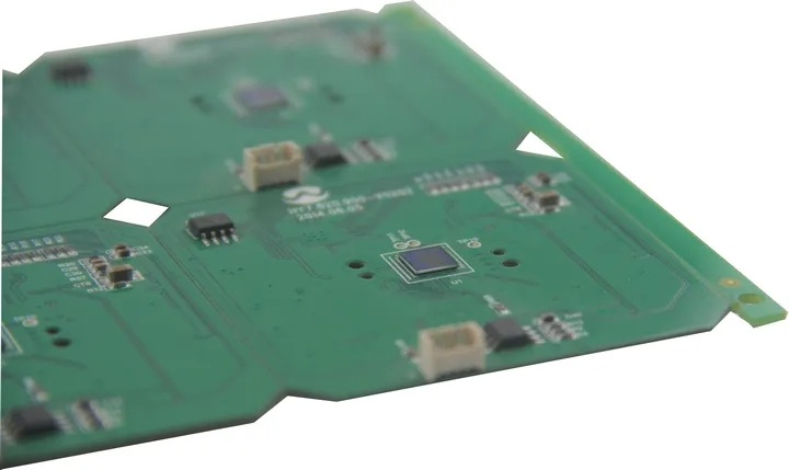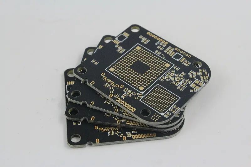
PCB manufacturers explain the design of PCB with blind holes
First of all, you should understand how the multilayer board is made, and understand how the holes are processed to make the PCB design of blind embedded holes. Now the multilayer board is generally composed of
A number of 2-layer plates are pressed together. For plates with only through holes, simply press several 2-layer plates together and then punch them
The size proportion design of the hole diameter: when the depth of the hole is more than 6 times of the hole diameter, it is impossible to ensure that the hole wall can be uniformly copper plated), and it is more troublesome to have blind holes
One point: for example, there are several processing methods for an 8-layer board 1-2 3-4 5-6 7-8 (here are 4 2-layer boards)
First, let's see how to do the first step

1) The simplest and most common way is to punch the four two-layer plates (i.e. blind buried holes), and there are 1-2 7-8 blind holes and 3-4 5-6 blind holes respectively
In this way, the two kinds of embedded holes can be pressed together and then punched. There will be 1-8 through holes. In this way, the pressing is only once. The production is simple and the cost is relatively high
Bottom Due to the different requirements of pcb lamination and the different distribution of routing layer, GND and Power layers, the first processing method cannot meet the design requirements
Yes, so we need to change the design and production
Now let's see how to do the second order
8. Such two kinds of blind holes and such two kinds of buried holes as 3-4 5-6. Then press (1-2+3-4) and punch, and there will be 1-4 blind holes. Then press Press and punch, there will be 5-8 blind holes. Press and punch the two 4-layer plates, and there will be 1-8 through holes. Although there are two kinds of holes
It has been pressed twice. The production is complicated and the defective rate is very high. Few factories are willing to do it
Some people think that I will only drill one or several blind buried holes, and it will not be expensive to go there, right? But in fact, due to the complete change of production mode, the cost is very low
More blind buried holes are almost the same
Some people design blind buried holes in a disorderly way. For example, they designed 1-6 and 3-8 holes for the above 8 layers. How can the factory press them when you design like this?
After 1-6, 3-8 holes cannot be made. Some people are even more excessive. They also design 1-3 and 5-7 holes. How do you want the factory to process them? Use 3 layers
Plate and 1 layer of plate?
I believe it will be helpful if you read it
In protel99se, after pressing O+K, there is a Drill Pairs button in the lower right corner, where you can set drill pairs, so that you can route and change
The software will automatically add the blind buried hole for you as long as the setting of the hole pair in the layer is satisfied. PCB design and PCB processing manufacturers introduce the PCB design of blind holes. Understand how to process those holes to make a PCB design of blind holes.


