
Professional PCB manufacturing and assembly
Building 6, Zone 3, Yuekang Road,Bao'an District, Shenzhen, China
+86-13410863085Mon.-Sat.08:00-20:00

PCB designers share their experience in PCB design with BGA devices
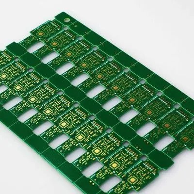
BGA is a commonly used component on PCB. PCB manufacturers share PCB design experience with BGA devices
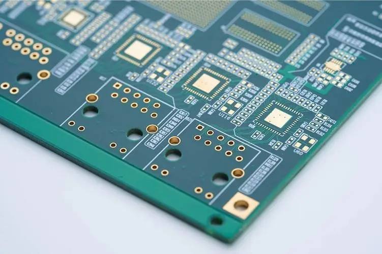
BGA is a commonly used component on PCB. Generally, CPU, NORTH BRIDGE, SOUTH BRIDGE, AGP CHIP, CARD BUS CHIP, etc. are mostly packaged in bga. In short, 80% of high-frequency signals and special signals will be pulled out of this type of package. Therefore, how to handle the routing of BGA packages will have a great impact on important signals.
Small parts usually surrounding BGA can be divided into several categories according to their importance:
by pass。
2. RC circuit of clock terminal.
(Appears in the form of series resistance and row group; for example, memory BUS signal)
4. EMI RC circuit (appearing in the form of "damp", "C" and "pull height"; for example, USB signal).
5. Other special circuits (special circuits added according to different CHIPs; such as CPU temperature sensing circuit).
6. Small power supply circuit group below 40 mil (in the form of C, L, R, etc.; this circuit often appears near AGP CHIP or CHIP with AGP function, and different power supply groups are separated through R and L).
7. pull low R、C。
8. General small circuit group (R, C, Q, U, etc.; no wiring requirements).
9.pull height R、RP。
The circuits of items 1-6 are usually the focus of placement, and they will be arranged as close to BGA as possible, which needs special treatment. The circuit of item 7 takes the second place in importance, but it will also be arranged closer to BGA. 8. Item 9 is a general circuit, which belongs to connecting existing signals.
Compared with the importance priority of small parts near BGA, the requirements on ROUTING are as follows:</SPAN<a>
. by pass=>When it is on the same side as the CHIP, it is directly connected by the CHIP pin to the by pass, and then pulled out by the by pass to connect via to the plane; When it is different from CHIP, it can share the same via with VCC and GND pin of BGA, and the line length should not exceed 100ml.
2. RC circuit of clock terminal=>There are requirements for line width, line spacing, line length or package GND; The routing shall be as short and smooth as possible and shall not cross the VCC separation line.
3. damping =>
There are requirements for line width, line spacing, line length and group routing; The routing shall be as short and smooth as possible, one group at a time, and other signals shall not be mixed.
4. EMI RC circuit=>There are line width, line spacing, parallel routing, package GND and other requirements; Complete according to customer requirements.
5. Other special circuits=>There are requirements for line width, package GND or wiring clearance; Complete according to customer requirements.
6. Small power supply circuit group below 40ml=>wire width and other requirements; The surface layer shall be used as far as possible, the inner space shall be reserved completely for the use of signal lines, and the power signal shall not pass through the BGA area to cause unnecessary interference.
7. Pull low R, C=>No special requirements; The wiring is smooth. PCB assembly, PCB design and PCB processing manufacturers explain that PCB designers share PCB design experience with BGA devices.


Just upload Gerber files, BOM files and design files, and the KINGFORD team will provide a complete quotation within 24h.