
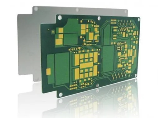
Professional PCB manufacturing and assembly
Building 6, Zone 3, Yuekang Road,Bao'an District, Shenzhen, China
+86-13410863085Mon.-Sat.08:00-20:00

The Function of PCB Stack Design and Circuit Measures
PCB manufacturers explain in detail the basic principles of PCB stack design and the role of circuit measures in PCB design
In PCB design, considering signal quality control factors, the general principles of PCB stack setting are as follows:
1. The second layer adjacent to the element surface is the ground plane, which provides the device shielding layer and the reference plane for the top layer wiring.
2. All signal layers shall be adjacent to the ground as much as possible to ensure a complete return channel.
3. Try to avoid two signal layers directly adjacent to each other to reduce crosstalk.
4. The main power supply shall be adjacent to its corresponding ground as far as possible to form a planar capacitor and reduce the planar impedance of the power supply.
5. Considering the symmetry of laminated structure, it is conducive to warping control during plate making production.
The above are the general principles of stack design. In the actual stack design, the circuit board designer can reduce the spacing between the corresponding wiring layers and the reference plane by increasing the spacing between adjacent wiring layers, so as to control the crosstalk rate of wiring between layers. On the premise that two signal layers can be directly adjacent. For consumer products that pay more attention to cost, we can reduce the plane impedance by weakening the way that the power supply is adjacent to the ground plane, so as to minimize the wiring layer and reduce PCB cost. Of course, the cost of this is the risk of signal quality design.
For the stack design of backplanes (Backplane or midplane), it is difficult for common backplanes to make adjacent routes perpendicular to each other, which inevitably leads to parallel long-distance wiring. For high-speed backplanes, the general stacking principles are as follows:
1. The top and bottom surfaces are complete ground planes, forming a shielding cavity.
2. There is no parallel wiring between adjacent layers to reduce crosstalk, or the spacing between adjacent wiring layers is far greater than the reference plane spacing.
3. All signal layers shall be adjacent to the ground as much as possible to ensure a complete return channel.
It should be noted that the above principles should be flexibly applied to PCB design and reasonable analysis should be made according to the actual board needs when setting specific PCB stacks.
Function of Circuit Measures in PCB Design
When designing electronic circuits, more attention is paid to the actual performance of the product, rather than to the electromagnetic compatibility characteristics, electromagnetic interference suppression and electromagnetic anti-interference characteristics of the product. In order to achieve its compatibility, the following circuit measures can be adopted in the actual PCB design:
(1) A high-frequency decoupling capacitor is set for each integrated circuit. A small high-frequency bypass capacitor shall be added beside each electrolytic capacitor.
(2) Use high-capacity tantalum capacitor or polyester capacitor instead of electrolytic capacitor as the charging and discharging energy storage capacitor on the circuit board. When using tubular capacitors, the shell should be grounded
(3) The signal entering the PCB shall be filtered, and the signal from the high noise area to the low noise area shall also be filtered. At the same time, the serial terminal resistance shall be used to reduce the signal reflection.
(4) The useless end of MCU shall be connected to power supply or ground through corresponding matching resistance. Or defined as an output terminal, the power and ground terminals on the integrated circuit should be connected, not suspended
(5) The unused gate circuit input terminal shall not be suspended, but connected to the power supply or ground through the corresponding matching resistance. The positive input terminal of the idle operational amplifier is grounded, and the negative input terminal is connected to the output terminal.
(6) Try to provide some form of damping (high-frequency capacitor, reverse diode, etc.) for relays, etc.
(7) A resistor can be connected in series on the PCB wiring to reduce the jump rate of the lower edge of the control signal wire.
TIPS: In order to achieve the goal of compatibility when using circuit schematic diagram for PCB design layout, necessary circuit measures must be taken to improve the electromagnetic compatibility of its products. Would you do the same for the siege lions? PCB manufacturers explain in detail the basic principles of PCB stack design and the role of circuit measures in PCB design.


Just upload Gerber files, BOM files and design files, and the KINGFORD team will provide a complete quotation within 24h.