
Professional PCB manufacturing and assembly
Building 6, Zone 3, Yuekang Road,Bao'an District, Shenzhen, China
+86-13410863085Mon.-Sat.08:00-20:00

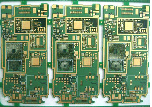
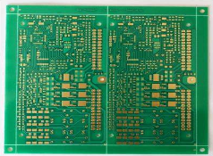
High frequency RF board laminated structure and wiring requirements
The circuit board manufacturer, circuit board designer and PCBA manufacturer will explain the stacking structure and wiring requirements of high-frequency RF boards
1、 High frequency RF board laminated structure
In addition to the impedance of the RF signal line, the stack structure of RF PCB RF boards also needs to consider heat dissipation, current, components, EMC, structure and skin effect. Generally, we follow the following basic principles in the layering and stacking of multilayer RF boards:
① Each layer of RF PCB high frequency RF board has a large area of floor, and there is no power plane. The adjacent two layers above and below the RF wiring layer should be ground planes.
Even if it is a digital analog mixed board, the digital part can have a power plane, but the RF area still needs to meet the requirements of large area paving on each floor.
B) For high power and high current RF boards, the RF main link should be placed on the top layer and connected with a wide microstrip line.
This is conducive to heat dissipation, reducing energy loss and reducing wire corrosion error.
② The power plane of the digital part shall be close to the grounding plane and arranged below the grounding plane.
In this way, the capacitance between the two metal plates can be used as the smoothing capacitance of the power supply, and the grounding plane can also shield the radiated current distributed on the power supply plane.
③ For the RF high-frequency RF board backplane, the upper and lower surface layers are both ground. In order to reduce the impedance discontinuity caused by vias and connectors, the second, third, fourth and fifth layers use digital signals.
The other stripline layers near the bottom are bottom signal layers. Similarly, the adjacent two layers above and below the RF signal layer should be the ground, and each layer should be paved in a large area.
④ For RF RF double-sided boards, the top layer is the signal layer and the bottom layer is the ground plane.
The RF board has four layers. The top layer is the signal layer, the second and fourth layers are ground planes, and the third layer uses power and control lines. In special cases, some RF signal lines can be used on the third layer. More layers of RF boards, and so on.
The specific stacking method and plane division requirements can refer to the 20050818 Printed Circuit Board Design Specification - EMC Requirements issued by EDA Design Department, and the online standard shall prevail.
2、 High frequency RF board wiring requirements
2.1 Corner
If the RF signal is routed at right angles, the effective line width at the corner will increase, and the impedance will be discontinuous, causing reflection. Therefore, there are mainly two methods for corner treatment: chamfer and fillet.
(1) The radius of the arc angle shall be large enough, generally speaking, R>3W.
(2) Chamfer is applicable to small corners, and the applicable frequency of chamfer can reach 10GHz.
2.2 Ribbon wiring
RF signals sometimes pass through the middle layer of the high-frequency RF board of the PCB, usually from the third layer. The second and fourth layers must be complete grounding planes, that is, eccentric stripline structures. The structural integrity of the stripline shall be ensured. The following requirements shall be met:
(1) The RF stripline is prohibited to span the ground plane gap of the upper and lower layers.
(2) The edges on both sides of the stripline shall be at least 3W wide from the edge of the upper and lower ground planes, and there shall be no ungrounded through holes within the range of 3W.
(3) It is recommended that the distance between the edge of the ground clad copper sheet and the edge of the stripline should be no less than 1.5W or 3H. H represents the total thickness of the dielectric layer below the stripline.
(4) The strip lines in the same layer shall be treated with ground clad copper sheet and ground through holes shall be added on the ground copper sheet with hole spacing less than λ/ 20. Evenly arrange in order. The edge of ground copper foil shall be smooth and flat, and no sharp burrs are allowed.
(5) If the stripline is to transmit high-power signals, in order to avoid 50 ohm line width being too thin, the copper sheet on the upper and lower reference planes of the stripline area should be hollowed out. The hollowing width is more than 5 times of the total dielectric thickness of the stripline. If the line width still cannot meet the requirements, the upper and lower adjacent second layer reference planes should be hollowed out.
2.3 Microstrip wiring
The top layer of the PCB RF board passes the RF signal, and the plane layer below the RF signal must be a complete grounding plane to form a microstrip line structure. To ensure the structural integrity of the microstrip line, the following requirements are required:
(1) RF signal routing is prohibited to cross the ground plane gap on the second floor.
(2) The distance between the microstrip line and the shielding wall shall be more than 2W. (Note: W is the line width).
(3) The edges on both sides of the microstrip line shall be at least 3W wide from the edge of the ground plane below. In the range of 3W, there shall be no ungrounded via.
The edge of ground copper foil shall be smooth and flat, and no sharp burrs are allowed. It is recommended that the edge of the ground clad copper sheet be no less than 1.5W wide or 3H wide from the edge of the microstrip line, and H represents the thickness of the microstrip substrate medium.
(4) The uncoupled microstrip line in the same layer shall be treated with ground clad copper sheet and ground via shall be added on the ground copper sheet, and the hole spacing shall be less than λ/ 20. Evenly arrange in order. PCB manufacturers, PCB designers and PCBA manufacturers will explain the stacking structure and wiring requirements of high-frequency RF boards.


Just upload Gerber files, BOM files and design files, and the KINGFORD team will provide a complete quotation within 24h.