
Professional PCB manufacturing and assembly
Building 6, Zone 3, Yuekang Road,Bao'an District, Shenzhen, China
+86-13410863085Mon.-Sat.08:00-20:00

1、 Material input stage
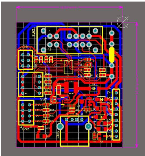
1. Whether the materials accepted in the process are complete (including schematic diagram, *. brd document, bill of materials, PCB design clarification, PCB design or change request, standardization request clarification, process design clarification document)
2. Confirm that the PCB template is up to date
3. Confirm that the position of the positioner of the template is correct
4. Can PCB design clarification, PCB design or change request, and standardization request clarification be understood
5. Confirm that the stop laying device and wiring area on the outline drawing have been shown on the PCB template
6. Compare the outline drawing to confirm that the dimensions and tolerances marked on the PCB are correct, and the definition of metallized holes and nonmetallic holes is accurate
7. After confirming that the PCB template is accurate, it is better to lock the construction file to avoid misoperation of the moved position
2、 Post planning inspection stage
a. Device inspection
8. Confirm whether the package of all devices can be different from the company's unified library, and whether the package library has been updated (check the operation results with the viewlog). If not, be sure to update Symbols
9. Motherboard and daughter board, single board and backplane, confirm that the signals and positions correspond, the connector direction and silk screen mark are correct, and the daughter board has anti misplug measures, and the components on the daughter board and motherboard should not interfere
10. Whether components can be placed 100%
11. Turn over the place ground of the TOP and BOTTOM layers of the device, and check whether the DRC caused by the stack is allowed
12. Is Mark point enough and necessary
13. Heavy components should be placed in the center near the PCB support point or edge to reduce PCB warpage
14. It is better to lock the components related to the structure after the layout to avoid misoperation of moving position
15. Within the range of 5mm around the crimping socket, no element with a height higher than the crimping socket is allowed on the front, and no element or solder joint is allowed on the back
16. Confirm whether the device planning can meet the process requirements (focus on BGA, PLCC and SMD socket)
17. For components with metal shell, pay special attention not to collide with other components, and leave enough space
18. The components related to the interface shall be placed as close to the interface as possible, and the backplane bus driver shall be placed as close to the backplane connector as possible
19. Can the CHIP device on the wave soldering surface ever be converted to wave soldering packaging,
20. Can the number of manual welding points exceed 50
21. Horizontal devices should be considered when installing high components on PCB axially. Leave room for lying. And consider the fixing method, such as the fixed pad of the crystal oscillator
22. For components requiring heat sink, confirm that there is enough space between them and other components, and pay attention to the height of main components within the range of heat sink
b. Function check
23. Whether the digital circuit and analog circuit components of the digital analog mixing board can be separated in the planning, and whether the signal flow is reasonable
24. The A/D converter is placed across the A/D partition.
25. Whether the clock device planning is reasonable
26. Whether the high-speed signal device planning is reasonable
27. Whether the termination devices have been properly placed (the source matching serial resistance should be placed at the driving end of the signal; the intermediate matching serial resistance should be placed at the middle position; the terminal matching serial resistance should be placed at the receiving end of the signal)
28. Whether the number and position of decoupling capacitors of IC devices are reasonable
29. The signal line takes the plane of different levels as the reference plane. When the plane division area is exceeded, whether the connecting capacitance between the reference planes can be close to the signal routing area.
30. Whether the planning of maintenance circuit is reasonable and conducive to division
31. Can the fuse of the single board power supply be placed near the connector without any circuit elements in front
32. Confirm that strong signal and weak signal (power difference of 30dB) circuits are laid separately
33. Whether the components that may affect the EMC experiment can be placed according to the design guide or the reference experience. For example, the reset circuit of the panel should be slightly close to the reset button
c. Fever
34. Heat sensitive components (including liquid medium capacitors and crystal oscillators) shall be kept away from high-power components, radiators and other heat sources as far as possible
35. Whether the planning can meet the thermal design request and the heat dissipation channel (according to the process design document)
D. Power supply
36. Can the IC power supply interval be too far from the IC
37. Whether the LDO and surrounding circuit planning are reasonable
38. Whether the circuit planning around the module power supply is reasonable
39. Whether the overall planning of power supply is reasonable
e. Rule Settings
40. Whether all simulation constraints have been correctly added to the Constraint Manager
41. Whether the physical and electrical rules can be set correctly (pay attention to the constraint settings of power network and ground network)
42. Is the spacing between Test Via and Test Pin sufficient
43. Can the thickness and plan of the stack meet the design and processing requirements
44. Whether all differential line impedances with characteristic impedance requests have been calculated and controlled by rules
3、 Post wiring inspection phase
e. Digital analog
45. Whether the routing of digital circuit and analog circuit can be separated, and whether the signal flow is reasonable
46. If A/D, D/A and similar circuits are separated from the ground, can the signal line between the circuits go from the bridge point between the two grounds (except the differential line)?
47. The signal line that must exceed the gap between the divided power supplies shall refer to the intact ground plane.
48. If the method of undivided stratigraphic design zoning is adopted, ensure that digital signals and analog signals are wired in zones.
F. Clock and high-speed local
49. Whether the impedance of each layer of high-speed signal line can persist in divergence
50. Can high-speed differential signal lines and similar signal lines be routed in parallel with equal length, symmetry and proximity?
51. Make sure that the clock line is in the inner layer as far as possible
52. Confirm whether the clock line, high-speed line, reset line and other strong radiation or sensitive lines can be routed according to the 3W standard line as far as possible
53. Is there no bifurcated test point on the clock, infix, reset signal, 100M/Gigabit Ethernet, and high-speed signal?
54. Can the low level signals such as LVDS and TTL/CMOS signals meet 10H as far as possible (H is the height of the signal line from the reference plane)?
55. Can the clock cable and high-speed signal cable prevent routing through the area of dense through-hole or device pins?
56. Can the clock line meet the (SI constraint) request (can the clock signal routing achieve less vias, short routing, and continuous reference planes, and the main reference plane should be GND as far as possible; if the GND main reference plane layer is changed during layer change, it is a GND vias within the range of 200mil from the vias)? If the main reference planes of different levels are changed during layer change, can there be decoupling capacitors within the range of 200mil from the vias)?
57. Whether the differential pair, high-speed signal line and various BUS can meet the (SI constraint) request
g. EMC and Reliability
58. Can we lay a layer of ground under the crystal oscillator? Can the signal wire be prevented from passing through the device pins? For high-speed sensitive devices, can the signal line be prevented from passing through the device pins?
59. There should be no acute angle or right angle on the signal wiring of the single board (generally continuous turning at an angle of 135 degrees, and the RF signal wiring should preferably be circular or chamfered copper foil after calculation)
60. For the double-sided PCB board, check whether the high-speed signal line and its return line can be wired together on the PCB; For multilayer boards, check whether the high-speed signal line can be routed as close to the ground plane as possible
61. For signal routing of adjacent two layers, try to route vertically
62. Prevent the signal line from crossing under the power module, common mode inductor, transformer and filter
63. Try to prevent long interval parallel wiring of high-speed signals on the same layer
64. Whether there are shielding vias on the edge of the board and the digital, analog and maintenance segmentation edges? Can multiple ground planes be connected by vias? Can the vias interval be less than 1/20 of the wavelength of the highest frequency signal?
65. Can the signal wiring corresponding to the surge suppression device be short and thick on the surface?
66. Confirm that the power supply and stratum are free of islands, excessive slotting, long ground surface cracks, thin strips and narrow channels caused by excessive through hole isolation disks or dense through holes
67. Whether the ground vias can be placed in the center where the signal lines span more layers (at least two ground planes are required)
h. Power and ground
68. If the power/ground plane is divided, try to prevent the high-speed signal from overstepping the divided reference plane.
69. Confirm that the power supply and ground can carry enough current. Whether the number of vias can meet the bearing requirements, (budget method: 1A/mm line width when the outer copper layer is 1oz thick, 0.5A/mm line width for the inner layer, and double the short line current)
70. Whether the power supply with special requirements can meet the voltage drop requirements
71. In order to reduce the edge radiation effect of the plane, the 20H criterion should be met as far as possible between the power layer and the stratum. (If conditions permit, the more indented the power layer, the better).
72. If there is division, can the divided land not form a loop?
73. Can different power planes of adjacent layers prevent overlapping?
74. Can the isolation of maintenance ground, - 48V ground and GND be greater than 2mm?
Can the 75, - 48V ground only return the - 48V signal without being connected to other ground? If not, please explain the reason in the remarks column.
76. Can a 10~20mm maintenance floor be arranged near the panel with connector, and double row interweave holes are used to connect the layers?
77. Can the spacing between PCB power lines and other signal lines meet the safety requirements?
i. Prohibited zone
78. There should be no PCB wiring, copper sheet and through-hole that may cause short circuit under metal shell devices and radiator components
79. There should be no wiring, copper sheet and through-hole around the device screw or washer that may cause short circuit
80. Can the reserved position in PCB design request be wired


Just upload Gerber files, BOM files and design files, and the KINGFORD team will provide a complete quotation within 24h.